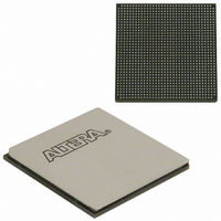
EP1AGX90EF1152I6N Altera, EP1AGX90EF1152I6N Datasheet - Page 105

EP1AGX90EF1152I6N
Manufacturer Part Number
EP1AGX90EF1152I6N
Description
IC ARRIA GX FPGA 90K 1152FBGA
Manufacturer
Altera
Series
Arria GXr
Datasheet
1.EP1AGX20CF484C6N.pdf
(234 pages)
Specifications of EP1AGX90EF1152I6N
Number Of Logic Elements/cells
90220
Number Of Labs/clbs
4511
Total Ram Bits
4477824
Number Of I /o
538
Voltage - Supply
1.15 V ~ 1.25 V
Mounting Type
Surface Mount
Operating Temperature
-40°C ~ 100°C
Package / Case
1152-FBGA
Lead Free Status / RoHS Status
Lead free / RoHS Compliant
Number Of Gates
-
Other names
544-2387
Available stocks
Company
Part Number
Manufacturer
Quantity
Price
- Current page: 105 of 234
- Download datasheet (4Mb)
Chapter 2: Arria GX Architecture
High-Speed Differential I/O with DPA Support
Table 2–29. Supported TDO/TDI Voltage Combinations
High-Speed Differential I/O with DPA Support
© December 2009 Altera Corporation
Arria GX
Non-Arria GX
Notes to
(1) The TDO output buffer meets V
(2) The TDO output buffer meets V
(3) An external 250- pull-up resistor is not required, but recommended if signal levels on the board are not optimal.
(4) Input buffer must be 3.3-V tolerant.
(5) Input buffer must be 2.5-V tolerant.
(6) Input buffer must be 1.8-V tolerant.
Device
Table
2–29:
Always V
Buffer Power
VCC = 3.3 V
VCC = 2.5 V
VCC = 1.8 V
VCC = 1.5 V
TDI Input
(3.3 V)
Arria GX devices contain dedicated circuitry for supporting differential standards at
speeds up to 840 Mbps. LVDS differential I/O standards are supported in the Arria
GX device. In addition, the LVPECL I/O standard is supported on input and output
clock pins on the top and bottom I/O banks.
The high-speed differential I/O circuitry supports the following high-speed I/O
interconnect standards and applications:
■
■
■
There are two dedicated high-speed PLLs (PLL1 and PLL2) in the EP1AGX20 and
EP1AGX35 devices and up to four dedicated high-speed PLLs (PLL1, PLL2, PLL7,
and PLL8) in the EP1AGX50, EP1AGX60, and EP1AGX90 devices to multiply
reference clocks and drive high-speed differential SERDES channels in I/O banks 1
and 2.
Table 2–30
in each of the Arria GX devices. In
transmitter or receiver provides the maximum number of channels that each fast PLL
can drive in its adjacent I/O bank (I/O Bank 1 or I/O Bank 2). The second row shows
the maximum number of channels that each fast PLL can drive in both I/O banks
(I/O Bank 1 and I/O Bank 2). For example, in the 780-pin FineLine BGA EP1AGX20
SPI-4 Phase 2 (POS-PHY Level 4)
SFI-4
Parallel RapidIO standard
C C P D
OH
OH
(MIN) = 2.4 V.
(MIN) = 2.0 V.
through
V
C C I O
v
v
v
v
v
(1),
(1),
(1),
= 3.3 V
(1)
(1)
(4)
(4)
(4)
Table 2–34
V
Arria GX TDO V
C C I O
v
v
v
v
v
list the number of channels that each fast PLL can clock
(2),
(2),
= 2.5 V
(2)
(2)
(2)
Table 2–30
(5)
(5)
C C I O
V
C C I O
Voltage Level in I/O Bank 4
v
v
v
v
through
v
= 1.8 V
(3)
(3)
(3)
(6)
Table 2–34
V
Level shifter
Level shifter
Level shifter
Level shifter
C C I O
required
required
required
required
Arria GX Device Handbook, Volume 1
v
= 1.5 V
the first row for each
V
Level shifter
Level shifter
Level shifter
Level shifter
C C I O
required
required
required
required
v
= 1.2 V
2–99
Related parts for EP1AGX90EF1152I6N
Image
Part Number
Description
Manufacturer
Datasheet
Request
R

Part Number:
Description:
CYCLONE II STARTER KIT EP2C20N
Manufacturer:
Altera
Datasheet:

Part Number:
Description:
CPLD, EP610 Family, ECMOS Process, 300 Gates, 16 Macro Cells, 16 Reg., 16 User I/Os, 5V Supply, 35 Speed Grade, 24DIP
Manufacturer:
Altera Corporation
Datasheet:

Part Number:
Description:
CPLD, EP610 Family, ECMOS Process, 300 Gates, 16 Macro Cells, 16 Reg., 16 User I/Os, 5V Supply, 15 Speed Grade, 24DIP
Manufacturer:
Altera Corporation
Datasheet:

Part Number:
Description:
Manufacturer:
Altera Corporation
Datasheet:

Part Number:
Description:
CPLD, EP610 Family, ECMOS Process, 300 Gates, 16 Macro Cells, 16 Reg., 16 User I/Os, 5V Supply, 30 Speed Grade, 24DIP
Manufacturer:
Altera Corporation
Datasheet:

Part Number:
Description:
High-performance, low-power erasable programmable logic devices with 8 macrocells, 10ns
Manufacturer:
Altera Corporation
Datasheet:

Part Number:
Description:
High-performance, low-power erasable programmable logic devices with 8 macrocells, 7ns
Manufacturer:
Altera Corporation
Datasheet:

Part Number:
Description:
Classic EPLD
Manufacturer:
Altera Corporation
Datasheet:

Part Number:
Description:
High-performance, low-power erasable programmable logic devices with 8 macrocells, 10ns
Manufacturer:
Altera Corporation
Datasheet:

Part Number:
Description:
Manufacturer:
Altera Corporation
Datasheet:

Part Number:
Description:
Manufacturer:
Altera Corporation
Datasheet:

Part Number:
Description:
Manufacturer:
Altera Corporation
Datasheet:

Part Number:
Description:
CPLD, EP610 Family, ECMOS Process, 300 Gates, 16 Macro Cells, 16 Reg., 16 User I/Os, 5V Supply, 25 Speed Grade, 24DIP
Manufacturer:
Altera Corporation
Datasheet:


