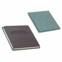
EP2S30F672I4 Altera, EP2S30F672I4 Datasheet - Page 230

EP2S30F672I4
Manufacturer Part Number
EP2S30F672I4
Description
IC STRATIX II FPGA 30K 672-FBGA
Manufacturer
Altera
Series
Stratix® IIr
Datasheet
1.EP2S15F484I4N.pdf
(238 pages)
Specifications of EP2S30F672I4
Number Of Logic Elements/cells
33880
Number Of Labs/clbs
1694
Total Ram Bits
1369728
Number Of I /o
500
Voltage - Supply
1.15 V ~ 1.25 V
Mounting Type
Surface Mount
Operating Temperature
-40°C ~ 100°C
Package / Case
672-FBGA
Family Name
Stratix II
Number Of Logic Blocks/elements
33880
# I/os (max)
500
Frequency (max)
711.24MHz
Process Technology
90nm (CMOS)
Operating Supply Voltage (typ)
1.2V
Logic Cells
33880
Ram Bits
1369728
Operating Supply Voltage (min)
1.15V
Operating Supply Voltage (max)
1.25V
Operating Temp Range
-40C to 100C
Operating Temperature Classification
Industrial
Mounting
Surface Mount
Pin Count
672
Package Type
FC-FBGA
Lead Free Status / RoHS Status
Contains lead / RoHS non-compliant
Number Of Gates
-
Lead Free Status / Rohs Status
Not Compliant
Other names
544-1899
EP2S30F672I4
EP2S30F672I4
Available stocks
Company
Part Number
Manufacturer
Quantity
Price
Company:
Part Number:
EP2S30F672I4
Manufacturer:
ALTERA
Quantity:
3 000
Company:
Part Number:
EP2S30F672I4N
Manufacturer:
ALTERA
Quantity:
238
External Memory Interface Specifications
External
Memory
Interface
Specifications
5–94
Stratix II Device Handbook, Volume 1
Tables 5–94
dedicated circuitry used for interfacing with external memory devices.
Table 5–95
Stratix II DQS delay buffer. Multiply the number of delay buffers that you
are using in the DQS logic block to get the maximum delay achievable in
your system. For example, if you implement a 90° phase shift at 200 MHz,
you use three delay buffers in mode 2. The maximum achievable delay
from the DQS block is then 3 × .416 ps = 1.248 ns.
Notes to
(1)
(2)
Table 5–94. DLL Frequency Range Specifications
Table 5–95. DQS Delay Buffer Maximum Delay in Fast Timing Model
Table 5–96. DQS Period Jitter Specifications for DLL-Delayed Clock
(tDQS_JITTER)
Number of DQS Delay Buffer
Frequency Mode
Frequency Mode
Peak-to-peak period jitter on the phase shifted DQS clock.
Delay stages used for requested DQS phase shift are reported in your project’s
Compilation Report in the Quartus II software.
Table
1, 2, 3
0
1
2
3
lists the maximum delay in the fast timing model for the
Stages
0
through
5–96:
1
2
3
4
(2)
Note (1)
5–101
240 to 350 (–4 and –5 speed grades)
Maximum Delay Per Delay Buffer
contain Stratix II device specifications for the
240 to 400 (–3 speed grade)
(Fast Timing Model)
Frequency Range
Commercial
100 to 175
150 to 230
200 to 310
110
130
160
0.833
0.416
80
Industrial
Altera Corporation
110
130
180
210
Resolution
(Degrees)
April 2011
22.5
Unit
30
30
36
36
ns
ns
Unit
ps
ps
ps
ps


