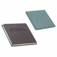
EP2S30F672I4 Altera, EP2S30F672I4 Datasheet - Page 144

EP2S30F672I4
Manufacturer Part Number
EP2S30F672I4
Description
IC STRATIX II FPGA 30K 672-FBGA
Manufacturer
Altera
Series
Stratix® IIr
Datasheet
1.EP2S15F484I4N.pdf
(238 pages)
Specifications of EP2S30F672I4
Number Of Logic Elements/cells
33880
Number Of Labs/clbs
1694
Total Ram Bits
1369728
Number Of I /o
500
Voltage - Supply
1.15 V ~ 1.25 V
Mounting Type
Surface Mount
Operating Temperature
-40°C ~ 100°C
Package / Case
672-FBGA
Family Name
Stratix II
Number Of Logic Blocks/elements
33880
# I/os (max)
500
Frequency (max)
711.24MHz
Process Technology
90nm (CMOS)
Operating Supply Voltage (typ)
1.2V
Logic Cells
33880
Ram Bits
1369728
Operating Supply Voltage (min)
1.15V
Operating Supply Voltage (max)
1.25V
Operating Temp Range
-40C to 100C
Operating Temperature Classification
Industrial
Mounting
Surface Mount
Pin Count
672
Package Type
FC-FBGA
Lead Free Status / RoHS Status
Contains lead / RoHS non-compliant
Number Of Gates
-
Lead Free Status / Rohs Status
Not Compliant
Other names
544-1899
EP2S30F672I4
EP2S30F672I4
Available stocks
Company
Part Number
Manufacturer
Quantity
Price
Company:
Part Number:
EP2S30F672I4
Manufacturer:
ALTERA
Quantity:
3 000
Company:
Part Number:
EP2S30F672I4N
Manufacturer:
ALTERA
Quantity:
238
Operating Conditions
5–8
Stratix II Device Handbook, Volume 1
Note to
(1)
V
V
V
V
V
R
V
V
V
V
V
R
Table 5–10. 2.5-V LVDS I/O Specifications
Table 5–11. 3.3-V LVDS I/O Specifications
Symbol
Symbol
CCIO
ID
ICM
OD
OCM
CCIO
ID
ICM
OD
OCM
L
L
The top and bottom clock input differential buffers in I/O banks 3, 4, 7, and 8 are powered by V
The PLL clock output/feedback differential buffers are powered by VCC_PLL_OUT. For differential clock
output/feedback operation, VCC_PLL_OUT should be connected to 3.3 V.
(1)
Table
I/O supply voltage for left and
right I/O banks (1, 2, 5, and
6)
Input differential voltage
swing (single-ended)
Input common mode voltage
Output differential voltage
(single-ended)
Output common mode
voltage
Receiver differential input
discrete resistor (external to
Stratix II devices)
I/O supply voltage for top
and bottom PLL banks (9,
10, 11, and 12)
Input differential voltage
swing (single-ended)
Input common mode voltage
Output differential voltage
(single-ended)
Output common mode
voltage
Receiver differential input
discrete resistor (external to
Stratix II devices)
5–11:
Parameter
Parameter
R
R
R
R
L
L
L
L
= 100 Ω
= 100 Ω
= 100 Ω
= 100 Ω
Conditions
Conditions
Minimum
Minimum
2.375
1.125
3.135
100
200
250
100
200
250
840
90
90
Typical
Typical
2.500
1,250
3.300
1,250
350
100
350
100
Altera Corporation
Maximum
Maximum
CCINT
2.625
1,800
1.375
3.465
1,800
1,570
900
450
110
900
710
110
, not V
April 2011
CCIO
Unit
Unit
mV
mV
mV
mV
mV
mV
mV
V
V
Ω
V
Ω
.


