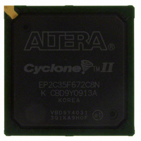
EP2C35F672C8N Altera, EP2C35F672C8N Datasheet - Page 34
EP2C35F672C8N
Manufacturer Part Number
EP2C35F672C8N
Description
IC CYCLONE II FPGA 33K 672-FBGA
Manufacturer
Altera
Series
Cyclone® IIr
Datasheet
1.EP2C5T144C8N.pdf
(168 pages)
Specifications of EP2C35F672C8N
Number Of Logic Elements/cells
33216
Number Of Labs/clbs
2076
Total Ram Bits
483840
Number Of I /o
475
Voltage - Supply
1.15 V ~ 1.25 V
Mounting Type
Surface Mount
Operating Temperature
0°C ~ 85°C
Package / Case
672-FBGA
No. Of Logic Blocks
2076
Family Type
Cyclone II
No. Of I/o's
475
I/o Supply Voltage
3.3V
Operating Frequency Max
320MHz
Operating Temperature Range
0°C To +85°C
Rohs Compliant
Yes
For Use With
NANO-CYCLONE - KIT NANOBOARD AND CYCLONEII DC807-1002 - DAUGHTER CARD ALTERA CYCLONE IIP0301 - DE2 CALL FOR ACADEMIC PRICING544-1733 - PCI KIT W/CYCLONE II EP2C35N
Lead Free Status / RoHS Status
Lead free / RoHS Compliant
Number Of Gates
-
Other names
544-1692
Available stocks
Company
Part Number
Manufacturer
Quantity
Price
Company:

Part Number:
EP2C35F672C8N
Manufacturer:
YAGEO
Quantity:
500 000
Company:
Part Number:
EP2C35F672C8N
Manufacturer:
ALTERA
Quantity:
500
Part Number:
EP2C35F672C8N
Manufacturer:
ALTERA/阿尔特拉
Quantity:
20 000


Global Clock Network & Phase-Locked Loops
Figure 2–13. Clock Control Block
Notes to
(1)
(2)
(3)
(4)
2–22
Cyclone II Device Handbook, Volume 1
CLK[n + 3]
CLK[n + 2]
CLK[n + 1]
CLK[n]
The CLKSWITCH signal can either be set through the configuration file or it can be dynamically set when using the
manual PLL switchover feature. The output of the multiplexer is the input reference clock (f
The CLKSELECT[1..0] signals are fed by internal logic and can be used to dynamically select the clock source for
the global clock network when the device is in user mode.
The static clock select signals are set in the configuration file and cannot be dynamically controlled when the device
is in user mode.
Internal logic can be used to enabled or disabled the global clock network in user mode.
Figure
2–13:
inclk1
inclk0
Static Clock Select (3)
CLKSWITCH (1)
Of the sources listed, only two clock pins, two PLL clock outputs, one
DPCLK pin, and one internally-generated signal are chosen to drive into a
clock control block.
clock control block. Out of these six inputs, the two clock input pins and
two PLL outputs can be dynamic selected to feed a global clock network.
The clock control block supports static selection of DPCLK and the signal
from internal logic.
f
IN
PLL
Internal Logic
DPCLK or
CDPCLK
C0
C1
C2
Figure 2–13
(3)
CLKSELECT[1..0] (2)
shows a more detailed diagram of the
Clock Control Block
Static Clock
Select (3)
CLKENA (4)
IN
Enable/
Disable
Altera Corporation
) for the PLL.
February 2007
Global
Clock
Related parts for EP2C35F672C8N
Image
Part Number
Description
Manufacturer
Datasheet
Request
R

Part Number:
Description:
CYCLONE II STARTER KIT EP2C20N
Manufacturer:
Altera
Datasheet:


Part Number:
Description:
CPLD, EP610 Family, ECMOS Process, 300 Gates, 16 Macro Cells, 16 Reg., 16 User I/Os, 5V Supply, 35 Speed Grade, 24DIP
Manufacturer:
Altera Corporation
Datasheet:
Part Number:
Description:
CPLD, EP610 Family, ECMOS Process, 300 Gates, 16 Macro Cells, 16 Reg., 16 User I/Os, 5V Supply, 15 Speed Grade, 24DIP
Manufacturer:
Altera Corporation
Datasheet:
Part Number:
Description:
Manufacturer:
Altera Corporation
Datasheet:
Part Number:
Description:
CPLD, EP610 Family, ECMOS Process, 300 Gates, 16 Macro Cells, 16 Reg., 16 User I/Os, 5V Supply, 30 Speed Grade, 24DIP
Manufacturer:
Altera Corporation
Datasheet:
Part Number:
Description:
High-performance, low-power erasable programmable logic devices with 8 macrocells, 10ns
Manufacturer:
Altera Corporation
Datasheet:
Part Number:
Description:
High-performance, low-power erasable programmable logic devices with 8 macrocells, 7ns
Manufacturer:
Altera Corporation
Datasheet:
Part Number:
Description:
Classic EPLD
Manufacturer:
Altera Corporation
Datasheet:
Part Number:
Description:
High-performance, low-power erasable programmable logic devices with 8 macrocells, 10ns
Manufacturer:
Altera Corporation
Datasheet:
Part Number:
Description:
Manufacturer:
Altera Corporation
Datasheet:
Part Number:
Description:
Manufacturer:
Altera Corporation
Datasheet:
Part Number:
Description:
Manufacturer:
Altera Corporation
Datasheet:
Part Number:
Description:
CPLD, EP610 Family, ECMOS Process, 300 Gates, 16 Macro Cells, 16 Reg., 16 User I/Os, 5V Supply, 25 Speed Grade, 24DIP
Manufacturer:
Altera Corporation
Datasheet: