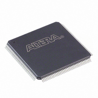
EP2C8T144C7N Altera, EP2C8T144C7N Datasheet - Page 42

EP2C8T144C7N
Manufacturer Part Number
EP2C8T144C7N
Description
IC CYCLONE II FPGA 8K 144-TQFP
Manufacturer
Altera
Series
Cyclone® IIr
Datasheet
1.EP2C5T144C8N.pdf
(168 pages)
Specifications of EP2C8T144C7N
Number Of Logic Elements/cells
8256
Number Of Labs/clbs
516
Total Ram Bits
165888
Number Of I /o
85
Voltage - Supply
1.15 V ~ 1.25 V
Mounting Type
Surface Mount
Operating Temperature
0°C ~ 85°C
Package / Case
144-TQFP, 144-VQFP
Lead Free Status / RoHS Status
Lead free / RoHS Compliant
Number Of Gates
-
Other names
544-1667
Available stocks
Company
Part Number
Manufacturer
Quantity
Price
Company:
Part Number:
EP2C8T144C7N
Manufacturer:
Altera
Quantity:
135
Company:
Part Number:
EP2C8T144C7N
Manufacturer:
ATLERA
Quantity:
10
Embedded Memory
2–30
Cyclone II Device Handbook, Volume 1
Memory Modes
Table 2–7
M4K memory blocks.
1
Single-port memory
Simple dual-port memory
Simple dual-port with mixed
width
True dual-port memory
True dual-port with mixed
width
Embedded shift register
ROM
FIFO buffers
Table 2–7. M4K Memory Modes
Memory Mode
Embedded Memory can be inferred in your HDL code or
directly instantiated in the Quartus II software using the
MegaWizard
summarizes the different memory modes supported by the
®
Plug-in Manager Memory Compiler feature.
M4K blocks support single-port mode, used when
simultaneous reads and writes are not required.
Single-port memory supports non-simultaneous
reads and writes.
Simple dual-port memory supports a
simultaneous read and write.
Simple dual-port memory mode with different
read and write port widths.
True dual-port mode supports any combination of
two-port operations: two reads, two writes, or one
read and one write at two different clock
frequencies.
True dual-port mode with different read and write
port widths.
M4K memory blocks are used to implement shift
registers. Data is written into each address
location at the falling edge of the clock and read
from the address at the rising edge of the clock.
The M4K memory blocks support ROM mode. A
MIF initializes the ROM contents of these blocks.
A single clock or dual clock FIFO may be
implemented in the M4K blocks. Simultaneous
read and write from an empty FIFO buffer is not
supported.
Description
Altera Corporation
February 2007


