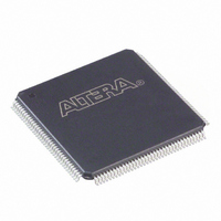
EP2C8T144C7N Altera, EP2C8T144C7N Datasheet - Page 53

EP2C8T144C7N
Manufacturer Part Number
EP2C8T144C7N
Description
IC CYCLONE II FPGA 8K 144-TQFP
Manufacturer
Altera
Series
Cyclone® IIr
Datasheet
1.EP2C5T144C8N.pdf
(168 pages)
Specifications of EP2C8T144C7N
Number Of Logic Elements/cells
8256
Number Of Labs/clbs
516
Total Ram Bits
165888
Number Of I /o
85
Voltage - Supply
1.15 V ~ 1.25 V
Mounting Type
Surface Mount
Operating Temperature
0°C ~ 85°C
Package / Case
144-TQFP, 144-VQFP
Lead Free Status / RoHS Status
Lead free / RoHS Compliant
Number Of Gates
-
Other names
544-1667
Available stocks
Company
Part Number
Manufacturer
Quantity
Price
Company:
Part Number:
EP2C8T144C7N
Manufacturer:
Altera
Quantity:
135
Company:
Part Number:
EP2C8T144C7N
Manufacturer:
ATLERA
Quantity:
10
- Current page: 53 of 168
- Download datasheet (3Mb)
Figure 2–23. Signal Path Through the I/O Block
Altera Corporation
February 2007
From Logic
To Logic
Array
Array
Row or Column
io_cce_out
io_clk[5..0]
io_dataout
io_datain0
io_datain1
io_cce_in
io_caclr
io_csclr
io_cclk
io_coe
The pin’s datain signals can drive the logic array. The logic array drives
the control and data signals, providing a flexible routing resource. The
row or column IOE clocks, io_clk[5..0], provide a dedicated routing
resource for low-skew, high-speed clocks. The global clock network
generates the IOE clocks that feed the row or column I/O regions (see
“Global Clock Network & Phase-Locked Loops” on page
Figure 2–23
Each IOE contains its own control signal selection for the following
control signals: oe, ce_in, ce_out, aclr/preset, sclr/preset,
clk_in, and clk_out.
selection.
Data and
Selection
Control
Signal
illustrates the signal paths through the I/O block.
oe
ce_in
ce_out
aclr/preset
sclr/preset
clk_in
clk_out
dataout
Figure 2–24
To Other
IOEs
Cyclone II Device Handbook, Volume 1
illustrates the control signal
IOE
Cyclone II Architecture
2–16).
2–41
Related parts for EP2C8T144C7N
Image
Part Number
Description
Manufacturer
Datasheet
Request
R

Part Number:
Description:
Cyclone Series Device Thermal Resistance
Manufacturer:
ALTERA [Altera Corporation]
Datasheet:

Part Number:
Description:
CYCLONE II STARTER KIT EP2C20N
Manufacturer:
Altera
Datasheet:

Part Number:
Description:
CPLD, EP610 Family, ECMOS Process, 300 Gates, 16 Macro Cells, 16 Reg., 16 User I/Os, 5V Supply, 35 Speed Grade, 24DIP
Manufacturer:
Altera Corporation
Datasheet:

Part Number:
Description:
CPLD, EP610 Family, ECMOS Process, 300 Gates, 16 Macro Cells, 16 Reg., 16 User I/Os, 5V Supply, 15 Speed Grade, 24DIP
Manufacturer:
Altera Corporation
Datasheet:

Part Number:
Description:
Manufacturer:
Altera Corporation
Datasheet:

Part Number:
Description:
CPLD, EP610 Family, ECMOS Process, 300 Gates, 16 Macro Cells, 16 Reg., 16 User I/Os, 5V Supply, 30 Speed Grade, 24DIP
Manufacturer:
Altera Corporation
Datasheet:

Part Number:
Description:
High-performance, low-power erasable programmable logic devices with 8 macrocells, 10ns
Manufacturer:
Altera Corporation
Datasheet:

Part Number:
Description:
High-performance, low-power erasable programmable logic devices with 8 macrocells, 7ns
Manufacturer:
Altera Corporation
Datasheet:

Part Number:
Description:
Classic EPLD
Manufacturer:
Altera Corporation
Datasheet:

Part Number:
Description:
High-performance, low-power erasable programmable logic devices with 8 macrocells, 10ns
Manufacturer:
Altera Corporation
Datasheet:

Part Number:
Description:
Manufacturer:
Altera Corporation
Datasheet:

Part Number:
Description:
Manufacturer:
Altera Corporation
Datasheet:

Part Number:
Description:
Manufacturer:
Altera Corporation
Datasheet:


