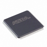
EP2C8T144C7N Altera, EP2C8T144C7N Datasheet - Page 76

EP2C8T144C7N
Manufacturer Part Number
EP2C8T144C7N
Description
IC CYCLONE II FPGA 8K 144-TQFP
Manufacturer
Altera
Series
Cyclone® IIr
Datasheet
1.EP2C5T144C8N.pdf
(168 pages)
Specifications of EP2C8T144C7N
Number Of Logic Elements/cells
8256
Number Of Labs/clbs
516
Total Ram Bits
165888
Number Of I /o
85
Voltage - Supply
1.15 V ~ 1.25 V
Mounting Type
Surface Mount
Operating Temperature
0°C ~ 85°C
Package / Case
144-TQFP, 144-VQFP
Lead Free Status / RoHS Status
Lead free / RoHS Compliant
Number Of Gates
-
Other names
544-1667
Available stocks
Company
Part Number
Manufacturer
Quantity
Price
Company:
Part Number:
EP2C8T144C7N
Manufacturer:
Altera
Quantity:
135
Company:
Part Number:
EP2C8T144C7N
Manufacturer:
ATLERA
Quantity:
10
IEEE Std. 1149.1 (JTAG) Boundary Scan Support
3–2
Cyclone II Device Handbook, Volume 1
SAMPLE/PRELOAD
EXTEST
BYPASS
USERCODE
IDCODE
HIGHZ
CLAMP
ICR
instructions
PULSE_NCONFIG
Table 3–1. Cyclone II JTAG Instructions (Part 1 of 2)
JTAG Instruction
(1)
(1)
(1)
00 0000 0101
00 0000 1111
11 1111 1111
00 0000 0111
00 0000 0110
00 0000 1011
00 0000 1010
00 0000 0001
Instruction Code
Cyclone II devices also use the JTAG port to monitor the logic operation
of the device with the SignalTap
devices support the JTAG instructions shown in
Allows a snapshot of signals at the device pins to be captured and
examined during normal device operation, and permits an initial
data pattern to be output at the device pins. Also used by the
SignalTap II embedded logic analyzer.
Allows the external circuitry and board-level interconnects to be
tested by forcing a test pattern at the output pins and capturing test
results at the input pins.
Places the 1-bit bypass register between the
which allows the BST data to pass synchronously through selected
devices to adjacent devices during normal device operation.
Selects the 32-bit
TDI
out of
Selects the
allowing the
Places the 1-bit bypass register between the
which allows the BST data to pass synchronously through selected
devices to adjacent devices during normal device operation, while
tri-stating all of the I/O pins.
Places the 1-bit bypass register between the
which allows the BST data to pass synchronously through selected
devices to adjacent devices during normal device operation while
holding I/O pins to a state defined by the data in the boundary-scan
register.
Used when configuring a Cyclone II device via the JTAG port with
a USB Blaster
ByteBlasterMV
File via an embedded processor.
Emulates pulsing the
even though the physical pin is unaffected.
and
TDO
TDO
.
IDCODE
IDCODE
pins, allowing the
™
™
, ByteBlaster
download cable, or when using a Jam File or JBC
USERCODE
®
register and places it between
nCONFIG
to be serially shifted out of
II embedded logic analyzer. Cyclone II
Description
™
register and places it between the
II, MasterBlaster
USERCODE
pin low to trigger reconfiguration
Table
to be serially shifted
TDI
TDI
TDI
3–1.
Altera Corporation
™
TDO
or
and
and
and
February 2007
TDI
.
TDO
TDO
TDO
and
pins,
pins,
pins,
TDO
,


