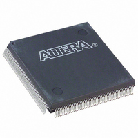
EP2C8Q208C8N Altera, EP2C8Q208C8N Datasheet - Page 56

EP2C8Q208C8N
Manufacturer Part Number
EP2C8Q208C8N
Description
IC CYCLONE II FPGA 8K 208-PQFP
Manufacturer
Altera
Series
Cyclone® IIr
Datasheet
1.EP2C5T144C8N.pdf
(168 pages)
Specifications of EP2C8Q208C8N
Number Of Logic Elements/cells
8256
Number Of Labs/clbs
516
Total Ram Bits
165888
Number Of I /o
138
Voltage - Supply
1.15 V ~ 1.25 V
Mounting Type
Surface Mount
Operating Temperature
0°C ~ 85°C
Package / Case
208-MQFP, 208-PQFP
Family Name
Cyclone® II
Number Of Logic Blocks/elements
8256
# I/os (max)
138
Frequency (max)
402.58MHz
Process Technology
90nm
Operating Supply Voltage (typ)
1.2V
Logic Cells
8256
Ram Bits
165888
Operating Supply Voltage (min)
1.15V
Operating Supply Voltage (max)
1.25V
Operating Temp Range
0C to 85C
Operating Temperature Classification
Commercial
Mounting
Surface Mount
Pin Count
208
Package Type
PQFP
Lead Free Status / RoHS Status
Lead free / RoHS Compliant
Number Of Gates
-
Lead Free Status / Rohs Status
Compliant
Other names
544-1671
Available stocks
Company
Part Number
Manufacturer
Quantity
Price
Company:
Part Number:
EP2C8Q208C8N
Manufacturer:
ALTERA
Quantity:
8
Company:
Part Number:
EP2C8Q208C8N
Manufacturer:
ALTERA
Quantity:
853
I/O Structure & Features
2–44
Cyclone II Device Handbook, Volume 1
Programmable delays can increase the register-to-pin delays for output
registers.
devices.
There are two paths in the IOE for an input to reach the logic array. Each
of the two paths can have a different delay. This allows you to adjust
delays from the pin to internal LE registers that reside in two different
areas of the device. You set the two combinational input delays by
selecting different delays for two different paths under the Input delay
from pin to internal cells logic option in the Quartus II software.
However, if the pin uses the input register, one of delays is disregarded
because the IOE only has two paths to internal logic. If the input register
is used, the IOE uses one input path. The other input path is then
available for the combinational path, and only one input delay
assignment is applied.
The IOE registers in each I/O block share the same source for clear or
preset. You can program preset or clear for each individual IOE, but both
features cannot be used simultaneously. You can also program the
registers to power up high or low after configuration is complete. If
programmed to power up low, an asynchronous clear can control the
registers. If programmed to power up high, an asynchronous preset can
control the registers. This feature prevents the inadvertent activation of
another device’s active-low input upon power up. If one register in an
IOE uses a preset or clear signal then all registers in the IOE must use that
same signal if they require preset or clear. Additionally a synchronous
reset signal is available for the IOE registers.
External Memory Interfacing
Cyclone II devices support a broad range of external memory interfaces
such as SDR SDRAM, DDR SDRAM, DDR2 SDRAM, and QDRII SRAM
external memories. Cyclone II devices feature dedicated high-speed
interfaces that transfer data between external memory devices at up to
167 MHz/333 Mbps for DDR and DDR2 SDRAM devices and
167 MHz/667 Mbps for QDRII SRAM devices. The programmable DQS
delay chain allows you to fine tune the phase shift for the input clocks or
strobes to properly align clock edges as needed to capture data.
Input pin to logic array delay
Input pin to input register delay
Output pin delay
Table 2–13. Cyclone II Programmable Delay Chain
Programmable Delays
Table 2–13
shows the programmable delays for Cyclone II
Input delay from pin to internal cells
Input delay from pin to input register
Delay from output register to output pin
Quartus II Logic Option
Altera Corporation
February 2007


