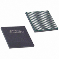
EPM2210F324C5N Altera, EPM2210F324C5N Datasheet - Page 57

EPM2210F324C5N
Manufacturer Part Number
EPM2210F324C5N
Description
IC MAX II CPLD 2210 LE 324-FBGA
Manufacturer
Altera
Series
MAX® IIr
Specifications of EPM2210F324C5N
Programmable Type
In System Programmable
Delay Time Tpd(1) Max
7.0ns
Voltage Supply - Internal
2.5V, 3.3V
Number Of Logic Elements/blocks
2210
Number Of Macrocells
1700
Number Of I /o
272
Operating Temperature
0°C ~ 85°C
Mounting Type
Surface Mount
Package / Case
324-FBGA
Voltage
2.5V, 3.3V
Memory Type
FLASH
Number Of Logic Elements/cells
2210
Family Name
MAX II
# Macrocells
1700
Frequency (max)
1.8797GHz
Propagation Delay Time
11.2ns
Number Of Logic Blocks/elements
221
# I/os (max)
272
Operating Supply Voltage (typ)
2.5/3.3V
In System Programmable
Yes
Operating Supply Voltage (min)
2.375V
Operating Supply Voltage (max)
3.6V
Operating Temp Range
0C to 85C
Operating Temperature Classification
Commercial
Mounting
Surface Mount
Pin Count
324
Package Type
FBGA
For Use With
P0305 - KIT MAX II MICRO
Lead Free Status / RoHS Status
Lead free / RoHS Compliant
Features
-
Lead Free Status / Rohs Status
Compliant
Other names
544-1961
EPM2210F324C5N
EPM2210F324C5N
Available stocks
Company
Part Number
Manufacturer
Quantity
Price
Company:
Part Number:
EPM2210F324C5N
Manufacturer:
ALTERA
Quantity:
453
Part Number:
EPM2210F324C5N
Manufacturer:
ALTERA/阿尔特拉
Quantity:
20 000
Chapter 4: Hot Socketing and Power-On Reset in MAX II Devices
Power-On Reset Circuitry
Figure 4–5. Power-Up Characteristics for MAX II, MAX IIG, and MAX IIZ Devices
Notes to
(1) Time scale is relative.
(2)
© October 2008 Altera Corporation
Figure 4–5
Figure
1.55 V
1.55 V
3.3 V
1.8 V
1.4 V
3.3 V
2.5 V
1.7 V
1.4 V
3.3 V
1.8 V
1.4 V
0 V
0 V
0 V
V
V
V
assumes all V
4–5:
CCINT
CCINT
CCINT
1
After SRAM configuration, all registers in the device are cleared and released into
user function before I/O tri-states are released. To release clears after tri-states are
released, use the DEV_CLRn pin option. To hold the tri-states beyond the power-up
configuration time, use the DEV_OE pin option.
CCIO
Tri-State
Tri-State
Tri-State
banks power up simultaneously with the V
t
t
t
CONFIG
CONFIG
CONFIG
MAX II Device
MAX IIG Device
MAX IIZ Device
Approximate Voltage
for SRAM Download Start
User Mode
User Mode
Operation
Operation
User Mode
Operation
minimum 10 µs
CCINT
profile shown. If not, t
V
Approximate Voltage
for SRAM Download Start
CCINT
Approximate Voltage
for SRAM Download Start
dips below this level
Tri-State
to 0 V if the V
must be powered down
Tri-State
Tri-State
CONFIG
(Note
CCINT
Device Resets
the SRAM and
Tri-States I/O Pins
stretches out until all V
Device Resets
the SRAM and
Tri-States I/O Pins
1),
(2)
t
User Mode
CONFIG
Operation
MAX II Device Handbook
CCIO
banks are powered.
4–7


