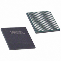
EPM2210F324C5N Altera, EPM2210F324C5N Datasheet - Page 38

EPM2210F324C5N
Manufacturer Part Number
EPM2210F324C5N
Description
IC MAX II CPLD 2210 LE 324-FBGA
Manufacturer
Altera
Series
MAX® IIr
Specifications of EPM2210F324C5N
Programmable Type
In System Programmable
Delay Time Tpd(1) Max
7.0ns
Voltage Supply - Internal
2.5V, 3.3V
Number Of Logic Elements/blocks
2210
Number Of Macrocells
1700
Number Of I /o
272
Operating Temperature
0°C ~ 85°C
Mounting Type
Surface Mount
Package / Case
324-FBGA
Voltage
2.5V, 3.3V
Memory Type
FLASH
Number Of Logic Elements/cells
2210
Family Name
MAX II
# Macrocells
1700
Frequency (max)
1.8797GHz
Propagation Delay Time
11.2ns
Number Of Logic Blocks/elements
221
# I/os (max)
272
Operating Supply Voltage (typ)
2.5/3.3V
In System Programmable
Yes
Operating Supply Voltage (min)
2.375V
Operating Supply Voltage (max)
3.6V
Operating Temp Range
0C to 85C
Operating Temperature Classification
Commercial
Mounting
Surface Mount
Pin Count
324
Package Type
FBGA
For Use With
P0305 - KIT MAX II MICRO
Lead Free Status / RoHS Status
Lead free / RoHS Compliant
Features
-
Lead Free Status / Rohs Status
Compliant
Other names
544-1961
EPM2210F324C5N
EPM2210F324C5N
Available stocks
Company
Part Number
Manufacturer
Quantity
Price
Company:
Part Number:
EPM2210F324C5N
Manufacturer:
ALTERA
Quantity:
453
Part Number:
EPM2210F324C5N
Manufacturer:
ALTERA/阿尔特拉
Quantity:
20 000
2–30
Slew-Rate Control
Open-Drain Output
Programmable Ground Pins
MAX II Device Handbook
Table 2–6. Programmable Drive Strength
The output buffer for each MAX II device I/O pin has a programmable output slew-
rate control that can be configured for low noise or high-speed performance. A faster
slew rate provides high-speed transitions for high-performance systems. However,
these fast transitions may introduce noise transients into the system. A slow slew rate
reduces system noise, but adds a nominal output delay to rising and falling edges.
The lower the voltage standard (for example, 1.8-V LVTTL) the larger the output
delay when slow slew is enabled. Each I/O pin has an individual slew-rate control,
allowing the designer to specify the slew rate on a pin-by-pin basis. The slew-rate
control affects both the rising and falling edges.
MAX II devices provide an optional open-drain (equivalent to open-collector) output
for each I/O pin. This open-drain output enables the device to provide system-level
control signals (for example, interrupt and write enable signals) that can be asserted
by any of several devices. This output can also provide an additional wired-OR plane.
Each unused I/O pin on MAX II devices can be used as an additional ground pin.
This programmable ground feature does not require the use of the associated LEs in
the device. In the Quartus II software, unused pins can be set as programmable GND
on a global default basis or they can be individually assigned. Unused pins also have
the option of being set as tri-stated input pins.
3.3-V LVTTL
3.3-V LVCMOS
2.5-V LVTTL/LVCMOS
1.8-V LVTTL/LVCMOS
1.5-V LVCMOS
Note to
(1) The I
is specified by the I/O standard. The I
maximum, where the V
condition is V
I/O Standard
Table
OH
current strength numbers shown are for a condition of a V
2–6:
OUT
= 1.7 V and the I
OL
maximum is specified by the I/O standard. For 2.5-V LVTTL/LVCMOS, the I
OL
condition is V
OL
current strength numbers shown are for a condition of a V
(Note 1)
IOH/IOL Current Strength Setting (mA)
OUT
= 0.7 V.
OUT
16
14
= V
8
8
4
7
6
3
4
2
OH
minimum, where the V
© October 2008 Altera Corporation
Chapter 2: MAX II Architecture
OH
minimum
OUT
OH
I/O Structure
= V
OL


