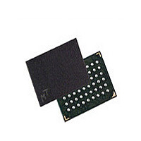
MT45W256KW16PEGA-70 WT Micron Technology Inc, MT45W256KW16PEGA-70 WT Datasheet - Page 5

MT45W256KW16PEGA-70 WT
Manufacturer Part Number
MT45W256KW16PEGA-70 WT
Description
Manufacturer
Micron Technology Inc
Datasheet
1.MT45W256KW16PEGA-70_WT.pdf
(28 pages)
Specifications of MT45W256KW16PEGA-70 WT
Operating Temperature (max)
85C
Mounting
Surface Mount
Operating Temperature Classification
Commercial
Lead Free Status / Rohs Status
Compliant
General Description
Functional Block Diagram
Figure 2:
PDF: 09005aef8329b746 / Source: 09005aef82f264aa
8mb_4mb_asyncpage_cr1_0_p22z__2.fm - Rev. B 4/08 EN
WE #
Functional Block Diagram - 256K x 16
OE #
UB #
CE #
LB #
ZZ #
Notes:
A[17:0]
Control
logic
Micron
power, portable applications. The MT45W256KW16PE is a 4Mb DRAM core device orga-
nized as 256K x 16 bits. These devices include the industry-standard, asynchronous
memory interface found on other low-power SRAM or pseudo-SRAM (PSRAM) offerings.
For seamless operation on an asynchronous memory bus, CellularRAM products incor-
porate a transparent self refresh mechanism. The hidden refresh requires no additional
support from the system memory controller and has no significant impact on device
read/write performance.
A user-accessible configuration register (CR) defines how the CellularRAM device
performs on-chip refresh and whether page mode read accesses are permitted. This
register is loaded automatically with a default setting during power-up and can be
updated at any time during normal operation.
Special attention has been focused on current consumption during self refresh. This
product includes two system-accessible mechanisms to minimize refresh current.
Setting sleep enable (ZZ#) to LOW enables one of two low-power modes: partial-array
refresh (PAR) or deep power-down (DPD). PAR limits refresh to only that part of the
DRAM array that contains essential data. DPD halts refresh operation altogether and is
used when no vital information is stored in the device. The system-configurable refresh
mechanisms are accessed through the CR.
1. Functional block diagrams illustrate simplified device operation. See the ball description
table, bus operations table, and timing diagrams for detailed information.
®
CellularRAM
Address decode
Configuration
register (CR)
logic
4Mb: 256K x16 Async/Page CellularRAM 1.0 Memory
®
products are high-speed, CMOS memories developed for low-
5
256K x 16
memory
Micron Technology, Inc., reserves the right to change products or specifications without notice.
DRAM
array
output
buffers
Input/
MUX
and
General Description
©2008 Micron Technology, Inc. All rights reserved.
DQ[7:0]
DQ[15:8]


