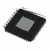
DAC1405D750HW/C1,5 NXP Semiconductors, DAC1405D750HW/C1,5 Datasheet - Page 24

DAC1405D750HW/C1,5
Manufacturer Part Number
DAC1405D750HW/C1,5
Description
IC DAC 14BIT SRL/SPI 100HTQFP
Manufacturer
NXP Semiconductors
Datasheet
1.DAC1405D750HWC15.pdf
(42 pages)
Specifications of DAC1405D750HW/C1,5
Settling Time
20ns
Number Of Bits
14
Data Interface
Serial, SPI™
Number Of Converters
2
Voltage Supply Source
Analog and Digital
Power Dissipation (max)
1.11W
Operating Temperature
-45°C ~ 85°C
Mounting Type
Surface Mount
Package / Case
100-TQFP Exposed Pad, 100-eTQFP, 100-HTQFP, 100-VQFP
Conversion Rate
750 MSPs
Resolution
14 bit
Interface Type
SPI
Supply Voltage (max)
3.6 V
Supply Voltage (min)
3 V
Maximum Operating Temperature
+ 85 C
Mounting Style
SMD/SMT
Maximum Power Dissipation
1.11 W
Minimum Operating Temperature
- 40 C
Supply Current
44 mA
Lead Free Status / RoHS Status
Lead free / RoHS Compliant
Other names
568-5089
Available stocks
Company
Part Number
Manufacturer
Quantity
Price
Company:
Part Number:
DAC1405D750HW/C1,5
Manufacturer:
IDT, Integrated Device Technology Inc
Quantity:
10 000
NXP Semiconductors
DAC1405D750
Product data sheet
10.4 Input clock
10.5 Timing
The DAC1405D750 can operate at the following clock frequencies:
The input clock is LVDS compliant (see
differential sine wave signal (see
The DAC1405D750 can operate at a sampling frequency (f
data rate (f
to the CLK signal. When the internal PLL is bypassed, the SYNC signal is used as a
reference. The input timing in the second case is shown in
when internal PLL bypassed
Fig 8.
Fig 9.
PLL on: up to 185 MHz in Dual-port mode and up to 370 MHz in Interleaved mode
PLL off: up to 750 MHz
LVDS clock configuration
Interfacing CML to LVDS
data
) up to 185 MHz. When using the internal PLL, the input data is referenced
All information provided in this document is subject to legal disclaimers.
L
Rev. 3 — 7 September 2010
Z
diff = 100 Ω
LVDS
Dual 14-bit DAC, up to 750 Msps; 4 and 8 interpolating
(off)”.
Z
diff
Figure
= 100 Ω
100 Ω
100 nF
100 nF
V
DDA(1V8)
AGND
Figure
9).
1.1 kΩ
2.2 kΩ
100 Ω
CLKN
CLKP
55 Ω
55 Ω
8) but it can also be interfaced with CML
100 nF
CLKN
CLKP
001aah021
Figure 10 “Input timing diagram
LVDS
s
DAC1405D750
) up to 750 Msps with an input
001aah020
LVDS
© NXP B.V. 2010. All rights reserved.
24 of 42


