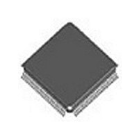
PEB20570FV3.1T Infineon Technologies, PEB20570FV3.1T Datasheet - Page 200

PEB20570FV3.1T
Manufacturer Part Number
PEB20570FV3.1T
Description
Manufacturer
Infineon Technologies
Datasheet
1.PEB20570FV3.1T.pdf
(308 pages)
Specifications of PEB20570FV3.1T
Lead Free Status / Rohs Status
Not Compliant
- Current page: 200 of 308
- Download datasheet (5Mb)
6.2.3
6.2.3.1
PCR Register
Reset value: 0000
PDR(1:0) PCM Data Rate
PDCL
PA
ICDB
SFH
Note: ’x’ = unused (read as ’0’)
Data Sheet
15
x
7
x
PCMU Register Description
PCMU Command Register
00 =
01 =
10 =
11 =
PCM Double Data Rate Clock
0 =
1 =
PCMU Activation
0 =
1 =
Idle Current D-Buffer
Used only for testing of PCMU in IDLE mode (PCR:PA = '0') to determine
which buffer is being accessed by the DSP
0 =
1 =
Second Frame Half
Applicable only in 16.384 Mbit/s data rate mode
0 =
1 =
H
14
x
6
x
2.048 Mbit/s (port 0..3)
4.096 Mbit/s (port 0, 2)
8.092 Mbit/s (port 0)
16.384 Mbit/s (1 x 256 time slots per frame, if only first or second
half of 8 kHz frame is handled) (port 0)
Single Data Rate Clock
Double Data Rate Clock
The PCMU is in idle mode
The PCMU is in active mode
Frame buffer 0 is accessed by the DSP
Frame buffer 1 is accessed by the DSP
The first 128 time slots of each frame are handled by the PCMU
The second 128 time slots of each frame are handled by the PCMU
SFH
13
5
x
ICDB
12
4
x
read/write
183
PA
11
x
3
PDCL
10
x
2
Register Description
Address: D060
9
1
x
PDR(1:0)
PEB 20570
PEB 20571
2003-07-31
8
0
x
H
Related parts for PEB20570FV3.1T
Image
Part Number
Description
Manufacturer
Datasheet
Request
R

Part Number:
Description:
ICs for Communications
Manufacturer:
Infineon Technologies AG
Datasheet:

Part Number:
Description:
Manufacturer:
Infineon Technologies AG
Datasheet:

Part Number:
Description:
Manufacturer:
Infineon Technologies AG
Datasheet:

Part Number:
Description:
Manufacturer:
Infineon Technologies AG
Datasheet:

Part Number:
Description:
Manufacturer:
Infineon Technologies AG
Datasheet:

Part Number:
Description:
Manufacturer:
Infineon Technologies AG
Datasheet:

Part Number:
Description:
Manufacturer:
Infineon Technologies AG
Datasheet:

Part Number:
Description:
Manufacturer:
Infineon Technologies AG
Datasheet:

Part Number:
Description:
16-bit microcontroller with 2x2 KByte RAM
Manufacturer:
Infineon Technologies AG
Datasheet:

Part Number:
Description:
NPN silicon RF transistor
Manufacturer:
Infineon Technologies AG
Datasheet:

Part Number:
Description:
NPN silicon RF transistor
Manufacturer:
Infineon Technologies AG
Datasheet:

Part Number:
Description:
NPN silicon RF transistor
Manufacturer:
Infineon Technologies AG
Datasheet:

Part Number:
Description:
NPN silicon RF transistor
Manufacturer:
Infineon Technologies AG
Datasheet:

Part Number:
Description:
Si-MMIC-amplifier in SIEGET 25-technologie
Manufacturer:
Infineon Technologies AG
Datasheet:

Part Number:
Description:
IGBT Power Module
Manufacturer:
Infineon Technologies AG
Datasheet:


