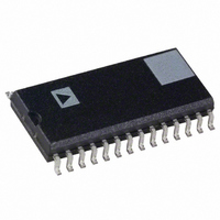
AD7564BR Analog Devices Inc, AD7564BR Datasheet - Page 7

AD7564BR
Manufacturer Part Number
AD7564BR
Description
IC DAC 12BIT LC2MOS QUAD 28-SOIC
Manufacturer
Analog Devices Inc
Datasheet
1.AD7564BRSZ.pdf
(16 pages)
Specifications of AD7564BR
Rohs Status
RoHS non-compliant
Settling Time
500ns
Number Of Bits
12
Data Interface
Serial
Number Of Converters
4
Voltage Supply Source
Single Supply
Power Dissipation (max)
50µW
Operating Temperature
-40°C ~ 85°C
Mounting Type
Surface Mount
Package / Case
28-SOIC (7.5mm Width)
Available stocks
Company
Part Number
Manufacturer
Quantity
Price
Part Number:
AD7564BRS
Manufacturer:
ADI/亚德诺
Quantity:
20 000
Part Number:
AD7564BRS-B
Manufacturer:
ADI/亚德诺
Quantity:
20 000
Company:
Part Number:
AD7564BRSZ
Manufacturer:
Maxim
Quantity:
456
Part Number:
AD7564BRSZ
Manufacturer:
ADI/亚德诺
Quantity:
20 000
Part Number:
AD7564BRSZ-REEL
Manufacturer:
ADI/亚德诺
Quantity:
20 000
Company:
Part Number:
AD7564BRZ
Manufacturer:
colour touch screen
Quantity:
100
Company:
Part Number:
AD7564BRZ
Manufacturer:
Analog Devices Inc
Quantity:
135
Part Number:
AD7564BRZ
Manufacturer:
ADI/亚德诺
Quantity:
20 000
REV. A
Pin
Number
1
2
3
4
5
6
7
8
9
10
11
12
13
14
15
16
17
18
19
20
21
22
23
24
25
26
27
28
Mnemonic
DGND
I
V
I
R
V
I
I
R
V
SDOUT
CLR
LDAC
FSIN
SDIN
CLKIN
A1
A0
V
R
I
I
V
R
I
N/C
AGND
I
OUT2
OUT1
OUT2
OUT1
OUT1
OUT2
OUT1
OUT2
DD
FB
REF
FB
REF
REF
FB
REF
FB
C
D
A
B
C
D
A
B
C
C
D
D
A
A
B
B
Description
Digital Ground.
I
Positive power supply. This is +5 V
I
Feedback resistor for DAC C.
DAC C reference input.
I
I
Feedback resistor for DAC D.
DAC D reference input.
This shift register output allows multiple devices to be connected in a daisy chain configuration.
Asynchronous CLR input. When this input is taken low, all DAC latches are loaded with all 0s.
Asynchronous LDAC input. When this input is taken low, all DAC latches are simultaneously
updated with the contents of the input latches.
Level-triggered control input (active low). This is the frame synchronization signal for the input data.
When FSIN goes low, it enables the input shift register, and data is transferred on the falling edges of
CLKIN. If the address bits are valid, the 12-bit DAC data is transferred to the appropriate input
latch on the sixteenth falling edge after FSIN goes low.
Serial data input. The device accepts a 16-bit word. DB0 and DB1 are DAC select bits. DB2 and
DB3 are device address bits. DB4 to DB15 contain the 12-bit data to be loaded to the selected
DAC.
Clock Input. Data is clocked into the input shift register on the falling edges of CLKIN.
Device address pin. This input in association with A0 gives the device an address. If DB2 and DB3
of the serial input stream do not correspond to this address, the data which follows is ignored and
not loaded to any input latch. However, it will appear at SDOUT irrespective of this.
Device address pin. This input in association with A1 gives the device an address.
DAC A reference input.
Feedback resistor for DAC A.
I
I
DAC B reference input.
Feedback resistor for DAC B.
I
No Connect pin.
This pin connects to the back gates of the current steering switches. It should be connected to the
signal ground of the system.
I
OUT2
OUT1
OUT2
OUT1
OUT1
OUT2
OUT1
OUT2
terminal for DAC C. This should normally connect to the signal ground of the system.
terminal for DAC C.
terminal for DAC D. This should normally connect to the signal ground of the system.
terminal for DAC D.
terminal for DAC A.
terminal for DAC A. This should normally connect to the signal ground of the system.
terminal for DAC B.
terminal for DAC B. This should normally connect to the signal ground of the system.
PIN DESCRIPTIONS
–7–
5%.
AD7564
3


