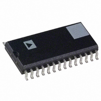
AD7564BR Analog Devices Inc, AD7564BR Datasheet

AD7564BR
Specifications of AD7564BR
Available stocks
Related parts for AD7564BR
AD7564BR Summary of contents
Page 1
FEATURES Four 12-Bit DACs in One Package 4-Quadrant Multiplication Separate References Single Supply Operation Guaranteed Specifications with +3.3 V/+5 V Supply Low Power Versatile Serial Interface Simultaneous Update Capability Reset Function 28-Pin SOIC, SSOP and DIP Packages APPLICATIONS Process ...
Page 2
AD7564–SPECIFICATIONS (V = +4. +5. Normal Mode unless otherwise noted) Parameter B Grade ACCURACY Resolution 12 Relative Accuracy 0.5 Differential Nonlinearity 0.5 Gain Error + MIN MAX 2 Gain ...
Page 3
Biased Mode T , unless otherwise noted) MAX Parameter ACCURACY Resolution Relative Accuracy Differential Nonlinearity Gain Error + MIN MAX 3 Gain Temperature Coefficient Output Leakage ...
Page 4
AD7564 AC Performance Characteristics (V = +4. +5. AD843 MIN Normal Mode not subject to test.) Parameter B Grade DYNAMIC PERFORMANCE Output Voltage Settling Time 550 Digital-to-Analog Glitch Impulse ...
Page 5
Timing Specifications ( Limit at Parameter +3 180 125 7 ...
Page 6
... Although the AD7564 features proprietary ESD protection circuitry, permanent damage may occur on devices subjected to high energy electrostatic discharges. Therefore, proper ESD precautions are recommended to avoid performance degradation or loss of functionality. Model AD7564BN AD7564BR AD7564BRS AD7564AR-B AD7564ARS DIP SOIC SSOP. DIP, SOIC and SSOP Packages + 0 ...
Page 7
Pin Number Mnemonic Description 1 DGND Digital Ground terminal for DAC C. This should normally connect to the signal ground of the system. OUT2 OUT2 3 V Positive power supply. This ...
Page 8
AD7564 TERMINOLOGY Relative Accuracy Relative accuracy or endpoint linearity is a measure of the maximum deviation from a straight line passing through the endpoints of the DAC transfer function measured after ad- justing for zero error and full-scale ...
Page 9
NORMAL MODE OF OPERATION 0.4 0.3 0.2 0.1 0 – Volts REF Figure 3. Differential Nonlinearity Error vs. V (Normal Mode 20V ...
Page 10
AD7564 2 AMP = AD820 1.6 V REF 1.4 1.2 1.0 0.8 0.6 0.4 0.2 0.0 0.2 0.4 0.6 0.8 1.0 |V – – Volts REF BIAS Figure 9. ...
Page 11
GENERAL DESCRIPTION D/A Section The AD7564 contains four 12-bit current output D/A convert- ers. A simplified circuit diagram for one of the D/A converters is shown in Figure 15. V REF ...
Page 12
AD7564 BIPOLAR OPERATION 4-Quadrant Multiplication) Figure 18 shows the standard connection diagram for bipolar operation of any one of the DACs in the AD7564. The coding is offset binary as shown in Table IV. When V the circuit performs 4-quadrant ...
Page 13
MICROPROCESSOR INTERFACING AD7564 to 80C51 Interface A serial interface between the AD7564 and the 80C51 micro- controller is shown in Figure 21. TXD of the 80C51 drives SCLK of the AD7564 while RXD drives the serial data line of the ...
Page 14
AD7564 AD7564 to ADSP-2101/ADSP-2103 Interface Figure 23 shows a serial interface between the AD7564 and the ADSP-2101/ADSP-2103 digital signal processors. The ADSP- 2101 operates from 5 V while the ADSP-2103 operates from 3 V supplies. These processors are set up ...
Page 15
APPLICATIONS Programmable State Variable Filter The AD7564 with its multiplying capability and fast settling time is ideal for many types of signal conditioning applications. The circuit of Figure 25 shows its use in a state variable filter design. This type ...
Page 16
AD7564 28 1 0.200 (5.080) MAX 0.020 (0.508) 0.015 (0.381) LEADS ARE SOLDER DIPPED OR TIN-PLATED ALLOY 42 OR COPPER. 28 0.299 (7.60) 0.291 (7.39) PIN 1 1 0.01 (0.254) 0.050 (1.27) 0.006 (0.15) 28 PIN 1 0.008 (0.203) 0.002 ...


