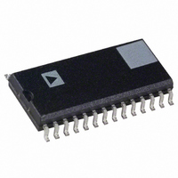
AD7564BR Analog Devices Inc, AD7564BR Datasheet - Page 13

AD7564BR
Manufacturer Part Number
AD7564BR
Description
IC DAC 12BIT LC2MOS QUAD 28-SOIC
Manufacturer
Analog Devices Inc
Datasheet
1.AD7564BRSZ.pdf
(16 pages)
Specifications of AD7564BR
Rohs Status
RoHS non-compliant
Settling Time
500ns
Number Of Bits
12
Data Interface
Serial
Number Of Converters
4
Voltage Supply Source
Single Supply
Power Dissipation (max)
50µW
Operating Temperature
-40°C ~ 85°C
Mounting Type
Surface Mount
Package / Case
28-SOIC (7.5mm Width)
Available stocks
Company
Part Number
Manufacturer
Quantity
Price
Part Number:
AD7564BRS
Manufacturer:
ADI/亚德诺
Quantity:
20 000
Part Number:
AD7564BRS-B
Manufacturer:
ADI/亚德诺
Quantity:
20 000
Company:
Part Number:
AD7564BRSZ
Manufacturer:
Maxim
Quantity:
456
Part Number:
AD7564BRSZ
Manufacturer:
ADI/亚德诺
Quantity:
20 000
Part Number:
AD7564BRSZ-REEL
Manufacturer:
ADI/亚德诺
Quantity:
20 000
Company:
Part Number:
AD7564BRZ
Manufacturer:
colour touch screen
Quantity:
100
Company:
Part Number:
AD7564BRZ
Manufacturer:
Analog Devices Inc
Quantity:
135
Part Number:
AD7564BRZ
Manufacturer:
ADI/亚德诺
Quantity:
20 000
REV. A
MICROPROCESSOR INTERFACING
AD7564 to 80C51 Interface
A serial interface between the AD7564 and the 80C51 micro-
controller is shown in Figure 21. TXD of the 80C51 drives
SCLK of the AD7564 while RXD drives the serial data line of
the part. The FSIN signal is derived from the port line P3.3.
The 80C51 provides the LSB of its SBUF register as the first bit
in the serial data stream. Therefore, the user will have to ensure
that the data in the SBUF register is arranged correctly so that
the data word transmitted to the AD7564 corresponds to the
loading sequence shown in Table I. When data is to be trans-
mitted to the part, P3.3 is taken low. Data on RXD is valid on
the falling edge of TXD. The 80C51 transmits its serial data in
8-bit bytes with only eight falling clock edges occurring in the
transmit cycle. To load data to the AD7564, P3.3 is left low
after the first eight bits are transferred and a second byte of data
is then transferred serially to the AD7564. When the second
serial transfer is complete, the P3.3 line is taken high. Note that
the 80C51 outputs the serial data byte in a format which has the
LSB first. The AD7564 expects the MSB first. The 80C51
transmit routine should take this into account.
LDAC and CLR on the AD7564 are also controlled by 80C51
port outputs. The user can bring LDAC low after every two
bytes have been transmitted to update the DAC which has been
programmed. Alternatively, it is possible to wait until all the in-
put registers have been loaded (sixteen byte transmits) and then
update the DAC outputs.
*ADDITIONAL PINS OMMITTED FOR CLARITY
80C51*
Figure 21. AD7564 to 80C51 Interface
P3.5
P3.4
P3.3
TXD
RXD
FSIN
CLR
LDAC
SDIN
SCLK
AD7564*
–13–
AD7564 to 68HC11 Interface
Figure 22 shows a serial interface between the AD7564 and the
68HC11 microcontroller. SCK of the 68HC11 drives SCLK of
the AD7564 while the MOSI output drives the serial data line of
the AD7564. The FSIN signal is derived from a port line
(PC7 shown).
For correct operation of this interface, the 68HC11 should be
configured such that its CPOL bit is a 0 and its CPHA bit is a 1.
When data is to be transmitted to the part, PC7 is taken low.
When the 68HC11 is configured like this, data on MOSI is valid
on the falling edge of SCK. The 68HC11 transmits its serial
data in 8-bit bytes (MSB first), with only eight falling clock
edges occurring in the transmit cycle. To load data to the
AD7564 , PC7 is left low after the first eight bits are transferred
and a second byte of data is then transferred serially to the
AD7564. When the second serial transfer is complete, the PC7
line is taken high.
In Figure 22, LDAC and CLR are controlled by the PC6
and PC5 port outputs. As with the 80C51, each DAC of the
AD7564 can be updated after each two-byte transfer, or else
all DACs can be simultaneously updated. This interface
is suitable for both 3 V and 5 V versions of the 68HC11
microcontroller.
*ADDITIONAL PINS OMMITTED FOR CLARITY
64HC11*
Figure 22. AD7564 to 64HC11 Interface
MOSI
SCK
PC5
PC6
PC7
LDAC
FSIN
CLR
SDIN
SCLK
AD7564*
AD7564
3


