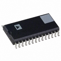
AD7564BR Analog Devices Inc, AD7564BR Datasheet - Page 4

AD7564BR
Manufacturer Part Number
AD7564BR
Description
IC DAC 12BIT LC2MOS QUAD 28-SOIC
Manufacturer
Analog Devices Inc
Datasheet
1.AD7564BRSZ.pdf
(16 pages)
Specifications of AD7564BR
Rohs Status
RoHS non-compliant
Settling Time
500ns
Number Of Bits
12
Data Interface
Serial
Number Of Converters
4
Voltage Supply Source
Single Supply
Power Dissipation (max)
50µW
Operating Temperature
-40°C ~ 85°C
Mounting Type
Surface Mount
Package / Case
28-SOIC (7.5mm Width)
Available stocks
Company
Part Number
Manufacturer
Quantity
Price
Part Number:
AD7564BRS
Manufacturer:
ADI/亚德诺
Quantity:
20 000
Part Number:
AD7564BRS-B
Manufacturer:
ADI/亚德诺
Quantity:
20 000
Company:
Part Number:
AD7564BRSZ
Manufacturer:
Maxim
Quantity:
456
Part Number:
AD7564BRSZ
Manufacturer:
ADI/亚德诺
Quantity:
20 000
Part Number:
AD7564BRSZ-REEL
Manufacturer:
ADI/亚德诺
Quantity:
20 000
Company:
Part Number:
AD7564BRZ
Manufacturer:
colour touch screen
Quantity:
100
Company:
Part Number:
AD7564BRZ
Manufacturer:
Analog Devices Inc
Quantity:
135
Part Number:
AD7564BRZ
Manufacturer:
ADI/亚德诺
Quantity:
20 000
AD7564
AC Performance Characteristics
Normal Mode
Parameter
DYNAMIC PERFORMANCE
AC Performance Characteristics
Biased Mode
Parameter
DYNAMIC PERFORMANCE
Output Voltage Settling Time
Digital-to-Analog Glitch Impulse
Multiplying Feedthrough Error
Output Capacitance
Channel-to-Channel Isolation
Digital Crosstalk
Digital Feedthrough
Total Harmonic Distortion
Output Noise Spectral Density
Output Voltage Settling Time
Digital to Analog Glitch Impulse
Multiplying Feedthrough Error
Output Capacitance
Digital Feedthrough
Total Harmonic Distortion
Output Noise Spectral Density
@ 1 kHz
@ 1 kHz
(V
output op amp is AD820; T
Guidance and are not subject to test.)
(V
AD843; T
not subject to test.)
DD
DD
= +3 V to +5.5 V; V
= +4.75 V to +5.25 V; V
A
= T
MIN
B Grade
550
35
–70
60
30
–76
5
5
–83
30
A Grade
3.5
35
–70
100
40
5
–76
20
to T
MAX
IOUT1
, unless otherwise noted. These characteristics are included for Design Guidance and are
A
= T
= V
IOUT1
Units
ns typ
nV-s typ
dB max
pF max
pF max
dB typ
nV-s typ
nV-s typ
dB typ
nV/ Hz typ
Units
nV-s typ
dB max
pF max
pF max
nV-s typ
dB typ
nV/ Hz typ
MIN
IOUT2
s typ
= V
to T
= 1.23 V; AGND = 0 V. V
IOUT2
MAX
, unless otherwise noted. These characteristics are included for Design
= AGND = 0 V. V
–4–
Test Conditions/Comments
To 0.01% of Full-Scale Range. DAC Latch Alternately Loaded
with All 0s and All 1s
Measured with V
with All 0s and All 1s
V
with All 0s
All 1s Loaded to DAC
All 0s Loaded to DAC
Feedthrough from Any One Reference to the Others with
20 V p-p, 10 kHz Sine Wave Applied
Effect of All 0s to All 1s Code Transition on Nonselected DACs
Feedthrough to Any DAC Output with FSIN High and Square
Wave Applied to SDIN and SCLK
V
All 1s Loaded to the DAC. V
ADOP07
Test Conditions/Comments
To 0.01% of Full-Scale Range. V
nately Loaded with all 0s and all 1s.
Measured with V
nately Loaded with all 0s and all 1s.
DAC Latch Loaded with all 0s.
All 1s Loaded to DAC
All 0s Loaded to DAC
Feedthrough to Any DAC Output with FSIN HIGH and a Square
Wave Applied to SDIN and CLKIN
All 1s Loaded to DAC. V
REF
REF
= 20 V p-p, 10 kHz Sine Wave. DAC Latch Loaded
= 6 V rms, 1 kHz Sine Wave
REF
REF
= 6 V rms, 1 kHz sine wave; DAC output op amp is
= 1 kHz, 2.45 V p-p, sine wave biased at 1.23 V; DAC
REF
IOUT2
= 0 V. DAC Register Alternately Loaded
= 0 V and V
IOUT2
REF
= 0 V; V
REF
= 0 V. Output Op Amp Is
REF
= 0 V. DAC Latch Alter-
= 0 V. DAC Register Alter-
REF
= 0 V
REV. A


