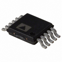
AD5063BRMZ Analog Devices Inc, AD5063BRMZ Datasheet - Page 3

AD5063BRMZ
Manufacturer Part Number
AD5063BRMZ
Description
IC DAC 16BIT 2.7-5.5V 10-MSOP
Manufacturer
Analog Devices Inc
Series
nanoDAC™r
Datasheet
1.AD5063BRMZ-REEL7.pdf
(20 pages)
Specifications of AD5063BRMZ
Data Interface
Serial, SPI™
Settling Time
4µs
Number Of Bits
16
Number Of Converters
1
Voltage Supply Source
Single Supply
Operating Temperature
-40°C ~ 85°C
Mounting Type
Surface Mount
Package / Case
10-MSOP, Micro10™, 10-uMAX, 10-uSOP
Resolution (bits)
16bit
Sampling Rate
333kSPS
Input Channel Type
Serial
Supply Voltage Range - Analog
2.7V To 5.5V
Supply Current
650µA
Digital Ic Case Style
SOP
Lead Free Status / RoHS Status
Lead free / RoHS Compliant
Power Dissipation (max)
-
Lead Free Status / RoHS Status
Lead free / RoHS Compliant, Lead free / RoHS Compliant
Available stocks
Company
Part Number
Manufacturer
Quantity
Price
Part Number:
AD5063BRMZ
Manufacturer:
ADI/亚德诺
Quantity:
20 000
SPECIFICATIONS
V
Table 2.
Parameter
STATIC PERFORMANCE
OUTPUT CHARACTERISTICS
REFERENCE INPUT/OUPUT
LOGIC INPUTS
DD
Resolution
Relative Accuracy (INL)
Total Unadjusted Error (TUE)
Differential Nonlinearity (DNL)
Gain Error
Gain Error Temperature Coefficient
Zero-Code Error
Zero-Code Error Temperature Coefficient
Offset Error
Offset Error Temperature Coefficient
Full-Scale Error
Bipolar Resistor Matching
Bipolar Zero Offset Error
Bipolar Zero Temperature Coefficient
Bipolar Gain Error
Output Voltage Range
Output Voltage Settling Time
Output Noise Spectral Density
Output Voltage Noise
Digital-to-Analog Glitch Impulse
Digital Feedthrough
DC Output Impedance (Normal)
DC Output Impedance (Power-Down)
V
Input Current (Power-Down)
Input Current (Normal)
DC Input Impedance
Input Current
Input Low Voltage, V
Input High Voltage, V
Pin Capacitance
REF
= 2.7 V to 5.5 V, V
(Output Connected to 1 kΩ Network)
(Output Connected to 10 kΩ Network)
AD5063BRMZ
AD5063BRMZ-1
Input Range
4
IL
REF
IH
= 4.096 V @ V
2
3
DD
= 5.0 V, R
16
0
−V
2.0
1.8
Min
2
REF
L
= unloaded, C
Typ
±0.5
±500
±0.5
±0.01
1
±0.05
0.05
±0.05
0.5
±500
1
±8
±0.5
±16
4
4
64
6
2
0.002
8
1
100
±1
1
±1
4
B Version
Rev. C | Page 3 of 20
Max
±1
±800
±1
±0.02
±0.1
±0.1
±800
±16
±32
V
V
1
V
±1
±2
0.8
0.8
REF
REF
DD
1
− 50 mV
L
= unloaded to GND; T
Unit
Bits
LSB
μV
LSB
% FSR
ppm FSR/°C
mV
μV/°C
mV
μV/°C
μV
Ω/Ω
LSB
ppm FSR/°C
LSB
V
V
μs
μs
μs
nV/√Hz
μV p-p
nV-s
nV-s
kΩ
kΩ
kΩ
μA
μA
MΩ
μA
V
V
pF
MIN
to T
Test Conditions/Comments
−40°C to + 85°C, B grade over all codes
Guaranteed monotonic
T
All 0s loaded to DAC register,
T
T
All 1s loaded to DAC register,
T
R
Unipolar operation
Bipolar operation
¼ scale to ¾ scale code transition to ±1 LSB
V
V
DAC code = midscale, 1 kHz
DAC code = midscale, 0.1 Hz to 10 Hz
bandwidth
1 LSB change around major carry
Output impedance tolerance ±10%
Output impedance tolerance ±400 Ω
Output impedance tolerance ±20 kΩ
Zero-scale loaded
Bipolar/unipolar operation
V
V
V
V
A
A
A
A
FB
DD
DD
DD
DD
DD
DD
= −40°C to +85°C
= −40°C to +85°C
= −40°C to +85°C
= −40°C to +85°C
/R
= 4.5 V to 5.5 V
= 2.7 V to 5.5 V
= 4.5 V to 5.5 V
= 2.7 V to 3.6 V
= 2.7 V to 5.5 V
= 2.7 V to 3.6 V
MAX
INV
, R
, unless otherwise noted.
FB
= R
INV
= 30 kΩ typically
AD5063


