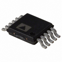
AD5063BRMZ Analog Devices Inc, AD5063BRMZ Datasheet - Page 13

AD5063BRMZ
Manufacturer Part Number
AD5063BRMZ
Description
IC DAC 16BIT 2.7-5.5V 10-MSOP
Manufacturer
Analog Devices Inc
Series
nanoDAC™r
Datasheet
1.AD5063BRMZ-REEL7.pdf
(20 pages)
Specifications of AD5063BRMZ
Data Interface
Serial, SPI™
Settling Time
4µs
Number Of Bits
16
Number Of Converters
1
Voltage Supply Source
Single Supply
Operating Temperature
-40°C ~ 85°C
Mounting Type
Surface Mount
Package / Case
10-MSOP, Micro10™, 10-uMAX, 10-uSOP
Resolution (bits)
16bit
Sampling Rate
333kSPS
Input Channel Type
Serial
Supply Voltage Range - Analog
2.7V To 5.5V
Supply Current
650µA
Digital Ic Case Style
SOP
Lead Free Status / RoHS Status
Lead free / RoHS Compliant
Power Dissipation (max)
-
Lead Free Status / RoHS Status
Lead free / RoHS Compliant, Lead free / RoHS Compliant
Available stocks
Company
Part Number
Manufacturer
Quantity
Price
Part Number:
AD5063BRMZ
Manufacturer:
ADI/亚德诺
Quantity:
20 000
THEORY OF OPERATION
The AD5063 is a single 16-bit, serial input, voltage-output DAC.
It operates from supply voltages of 2.7 V to 5.5 V. Data is
written to the AD5063 in a 24-bit word format via a 3-wire serial
interface.
The AD5063 incorporates a power-on reset circuit that ensures
the DAC output powers up to midscale. The device also has a
software power-down mode pin that reduces the typical current
consumption to less than 1 μA.
DAC ARCHITECTURE
The DAC architecture of the AD5063 consists of two matched
DAC sections. A simplified circuit diagram is shown in
Figure 27. The four MSBs of the 16-bit data-word are decoded
to drive 15 switches, E1 to E15. Each of these switches connects
one of 15 matched resistors to either the DACGND or V
buffer output. The remaining 12 bits of the data-word drive
Switches S0 to S11 of a 12-bit voltage mode R-2R ladder
network.
V
REFERENCE BUFFER
The AD5063 operates with an external reference. The reference
input (V
input voltage is used to provide a buffered reference for the
DAC core.
SERIAL INTERFACE
The AD5063 has a 3-wire serial interface ( SYNC , SCLK, and
DIN) that is compatible with SPI, QSPI, and MICROWIRE
interface standards, as well as most DSPs. (See
timing diagram of a typical write sequence.)
REF
0
0
2R
REF
) has an input range of 2 V to AV
12-BIT R-2R LADDER
2R
S0
0
Figure 27. DAC Ladder Structure
0
2R
S1
0
S11
2R
0
FOUR MSBs DECODED INTO
15 EQUAL SEGMENTS
PD1
2R
E1
PD0
2R
E2
DD
DB15 (MSB)
− 50 mV. This
Figure 2
D15
0
0
1
1
2R
E15
0
1
0
1
D14
Figure 28. Input Register Contents
for a
NORMAL OPERATION
THREE-STATE
100kΩ TO GND
1kΩ TO GND
REF
V
OUT
D13
Rev. C | Page 13 of 20
D12
D11
POWER-DOWN MODES
The write sequence begins by bringing the SYNC line low. Data
from the DIN line is clocked into the 24-bit shift register on the
falling edge of SCLK. The serial clock frequency can be as high
as 30 MHz, making these parts compatible with high speed
DSPs. On the 24
in and the programmed function is executed (that is, a change
in the DAC register contents and/or a change in the mode of
operation).
At this stage, the SYNC line can be kept low or be brought
high. In either case, it must be brought high for a minimum of
12 ns before the next write sequence, so that a falling edge of
SYNC can initiate the next write sequence. Because the SYNC
buffer draws more current when V
V
for even lower power operation of the part. As previously indi-
cated, however, it must be brought high again just before the
next write sequence.
INPUT SHIFT REGISTER
The input shift register is 24 bits wide (see Figure 28). PD1
and PD0 are bits that control the operating mode of the part
(normal mode or any one of the three power-down modes).
There is a more complete description of the various modes in
the Power-Down Modes section. The next 16 bits are the data
bits. These are transferred to the DAC register on the 24
edge of SCLK.
SYNC INTERRUPT
In a normal write sequence, the SYNC line is kept low for at
least 24 falling edges of SCLK, and the DAC is updated on the
24
24
The shift register is reset and the write sequence is seen as
invalid. Neither an update of the DAC register contents nor a
change in the operating mode occurs (see
IH
D10
th
th
= 0.8 V, SYNC should be idled low between write sequences
falling edge. However, if SYNC is brought high before the
falling edge, it acts as an interrupt to the write sequence.
D9
DATA BITS
D8
th
falling clock edge, the last data bit is clocked
D7
D6
D5
IH
D4
= 1.8 V than it does when
D3
Figure 31
D2
).
AD5063
D1
DB0 (LSB)
th
D0
falling


