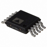
AD5063BRMZ Analog Devices Inc, AD5063BRMZ Datasheet - Page 16

AD5063BRMZ
Manufacturer Part Number
AD5063BRMZ
Description
IC DAC 16BIT 2.7-5.5V 10-MSOP
Manufacturer
Analog Devices Inc
Series
nanoDAC™r
Datasheet
1.AD5063BRMZ-REEL7.pdf
(20 pages)
Specifications of AD5063BRMZ
Data Interface
Serial, SPI™
Settling Time
4µs
Number Of Bits
16
Number Of Converters
1
Voltage Supply Source
Single Supply
Operating Temperature
-40°C ~ 85°C
Mounting Type
Surface Mount
Package / Case
10-MSOP, Micro10™, 10-uMAX, 10-uSOP
Resolution (bits)
16bit
Sampling Rate
333kSPS
Input Channel Type
Serial
Supply Voltage Range - Analog
2.7V To 5.5V
Supply Current
650µA
Digital Ic Case Style
SOP
Lead Free Status / RoHS Status
Lead free / RoHS Compliant
Power Dissipation (max)
-
Lead Free Status / RoHS Status
Lead free / RoHS Compliant, Lead free / RoHS Compliant
Available stocks
Company
Part Number
Manufacturer
Quantity
Price
Part Number:
AD5063BRMZ
Manufacturer:
ADI/亚德诺
Quantity:
20 000
AD5063
APPLICATIONS
CHOOSING A REFERENCE FOR THE AD5063
To achieve optimum performance of the AD5063, thought
should be given to the choice of a precision voltage reference.
The AD5063 has one reference input, V
reference input is used to supply the positive input to the DAC;
therefore, any error in the reference is reflected in the DAC.
There are four possible sources of error when choosing a voltage
reference for high accuracy applications: initial accuracy, ppm
drift, long-term drift, and output voltage noise. Initial accuracy
on the output voltage of the DAC leads to a full-scale error in the
DAC. To minimize these errors, a reference with high initial
accuracy is preferred. Also, choosing a reference with an output
trim adjustment, such as the ADR423, allows a system designer to
trim out system errors by setting a reference voltage to a voltage
other than the nominal. The trim adjustment can also be used at
any point within the operating temperature range to trim out error.
Because the supply current required by the AD5063 is extremely
low, the parts are ideal for low supply applications. The ADR395
voltage reference is recommended; it requires less than 100 μA of
quiescent current and can, therefore, drive multiple DACs in one
system, if required. It also provides very good noise performance
at 8 μV p-p in the 0.1 Hz to 10 Hz range.
Long-term drift is a measure of how much the reference drifts
over time. A reference with a tight long-term drift specification
ensures that the overall solution remains relatively stable during
its entire lifetime. The temperature coefficient of a reference’s
output voltage affects INL, DNL, and TUE. A reference with a
tight temperature coefficient specification should be chosen to
reduce the temperature dependence of the DAC output voltage
on ambient conditions.
In high accuracy applications, which have a relatively low
tolerance for noise, reference output voltage noise needs to be
considered. It is important to choose a reference with as low an
output noise voltage as practical for the system noise resolution
required. Precision voltage references, such as the ADR435,
produce low output noise in the 0.1 Hz to 10 Hz region. Exam-
ples of some recommended precision references for use as the
supply to the AD5063 are shown in Table 7.
INTERFACE
SERIAL
3-WIRE
SYNC
SCLK
Figure 36. ADR395 as a Reference to AD5063
7V
DIN
ADR395
5V
AD5063
REF
. The voltage on the
V
OUT
= 0V TO 5V
Rev. C | Page 16 of 20
Table 7. Recommended Precision References for the AD5063
Part No.
ADR435
ADR425
ADR02
ADR02
ADR395
BIPOLAR OPERATION USING THE AD5063
The AD5063 has been designed for single-supply operation, but
a bipolar output range is also possible by using the circuit shown
in Figure 37. This circuit yields an output voltage range of ±4.096 V.
Rail-to-rail operation at the amplifier output is achievable using
AD8675/AD8031/AD8032 or an OP196.
The output voltage for any input code can be calculated as
where D represents the input code in decimal (0 to 65,536).
With V
This is an output voltage range of ±5 V, with 0x0000 corresponding
to a −5 V output and 0xFFFF corresponding to a +5 V output.
INTERFACE
SERIAL
V
V
O
O
REF
=
=
= 5 V, R1 = R2 = 30 kΩ
0.1 µ F
⎡
⎢
⎣
⎛
⎜
⎝
Initial
Accuracy
(mV max)
±2
±2
±3
±3
±5
V
10
65536
SCLK
SYNC
DIN
DD
DACGND
+5V
V
×
DD
×
D
+4.096V
⎛
⎜
⎝
⎞
⎟
⎠
65
−
Figure 37. Bipolar Operation
0.1 µ F
V
REF
AD5063
D
,
5
536
AGND
V
Temperature Drift
(ppm/°C max)
3 (R-8)
3 (R-8)
3 (R-8)
3 (SC-70)
9 (TSOT-23)
10 µ F
+
⎞
× ⎟
⎠
R
INV
⎛
⎜
⎝
R1
R
R1
R
+
FB
FB
R2
OUT
⎞
⎟
⎠
INV
−
V
DD
EXTERNAL
0.1 Hz to 10 Hz
Noise (μV p-p typ)
8
3.4
10
10
8
⎛ ×
OP AMP
⎜
⎝
–5V
+5V
R2
R1
⎞
⎟
⎠
⎤
⎥
⎦
BIPOLAR
OUTPUT


