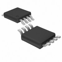
LTC1663IMS8 Linear Technology, LTC1663IMS8 Datasheet - Page 5

LTC1663IMS8
Manufacturer Part Number
LTC1663IMS8
Description
IC DAC 10BIT R-R MICROPWR 8MSOP
Manufacturer
Linear Technology
Datasheet
1.LTC1663CS5TRMPBF.pdf
(12 pages)
Specifications of LTC1663IMS8
Settling Time
30µs
Number Of Bits
10
Data Interface
Serial
Number Of Converters
1
Voltage Supply Source
Single Supply
Power Dissipation (max)
630µW
Operating Temperature
-40°C ~ 85°C
Mounting Type
Surface Mount
Package / Case
8-MSOP, Micro8™, 8-uMAX, 8-uSOP,
Lead Free Status / RoHS Status
Contains lead / RoHS non-compliant
Available stocks
Company
Part Number
Manufacturer
Quantity
Price
Company:
Part Number:
LTC1663IMS8
Manufacturer:
LT
Quantity:
5 321
Company:
Part Number:
LTC1663IMS8
Manufacturer:
LT
Quantity:
10 000
Part Number:
LTC1663IMS8
Manufacturer:
LINEAR/凌特
Quantity:
20 000
Company:
Part Number:
LTC1663IMS8#PBF
Manufacturer:
LINEAR
Quantity:
10
Part Number:
LTC1663IMS8#TR
Manufacturer:
LT/凌特
Quantity:
20 000
Company:
Part Number:
LTC1663IMS8#TRPBF
Manufacturer:
LINEAR
Quantity:
13 257
Part Number:
LTC1663IMS8#TRPBF
Manufacturer:
LINEAR/凌特
Quantity:
20 000
TYPICAL PERFORMANCE CHARACTERISTICS
PIN FUNCTIONS
SDA (Pin 1, Pin 1 on SOT-23): Serial Data Bidirectional
Pin. Data is shifted into the SDA pin and acknowledged
by the SDA pin. High impedance pin while data is shifted
in. Open-drain N-channel output during acknowledgment.
Requires a pull-up resistor or current source to V
AD1 (Pin 2): Slave Address Select Bit 1. Tie this pin to
either V
LTC1663’s slave address.
AD2 (Pin 3): Slave Address Select Bit 2. Tie this pin to
either V
LTC1663’s slave address.
DEFINITIONS
Differential Nonlinearity (DNL): The difference between
the measured change and the ideal 1LSB change for any
two adjacent codes. The DNL error between any two codes
is calculated as follows:
Where ΔV
two adjacent codes.
DNL = (ΔV
–0.2
–0.4
–0.6
–1.0
–0.8
1.0
0.8
0.6
0.4
0.2
0
–1.0
Load Regulation vs Output Current
V
V
CODE = 512
T
CC
CC
–0.8
A
CC
OUT
= 25°C
OUT
= V
or GND to modify the corresponding bit of the
or GND to modify the corresponding bit of the
= 1.5V
–0.6 –0.4
SOURCE
REF
OUT
is the measured voltage difference between
= 3V
–0.2
– LSB)/LSB
I
OUT
0 0.2
(mA)
0.4
SINK
0.6
0.8 1.0
1663 G07
–1
–2
–3
–4
–5
5
4
3
2
1
0
–60
Offset Error Voltage vs
Temperature
–40
CC
.
–20
TEMPERATURE (°C)
0
20
SCL (Pin 4, Pin 5 on SOT-23): Serial Clock Input Pin.
Data is shifted into the SDA pin at the rising edges of the
clock. This high impedance pin requires a pull-up resistor
or current source to V
V
≤ 5.5V. Also used as the reference voltage input when the
part is programmed to use V
AD0 (Pin 6): Slave Address Select Bit 0. Tie this pin to
either V
LTC1663’s slave address.
GND (Pin 7, Pin 2 on SOT-23): System Ground.
V
rail-to-rail DAC output.
Digital Feedthrough: The glitch that appears at the ana-
log output caused by AC coupling from the digital inputs
when they change state. The area of the glitch is specifi ed
in (nV)(sec).
Full-Scale Error (FSE): The deviation of the actual full-scale
voltage from ideal. FSE includes the effects of offset and
gain errors (see Applications Information).
CC
OUT
40
(Pin 5, Pin 4 on SOT-23): Power Supply. 2.7V ≤ V
(Pin 8, Pin 3 on SOT-23): Voltage Output. Buffered
60
CC
or GND to modify the corresponding bit of the
80
1663 G08
100
2.510
2.508
2.506
2.504
2.502
2.500
2.498
2.496
2.494
2.492
2.490
CC
.
–60
Full-Scale Output Voltage vs
Temperature
REFERENCE SET TO
INTERNAL BANDGAP
–40
CC
–20
as the reference.
TEMPERATURE (°C)
0
LTC1663
20
40
60
80
1663 G09
1663fd
5
100
CC


