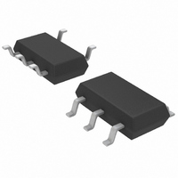
LTC1663-1CS5#TRMPBF Linear Technology, LTC1663-1CS5#TRMPBF Datasheet

LTC1663-1CS5#TRMPBF
Specifications of LTC1663-1CS5#TRMPBF
Available stocks
Related parts for LTC1663-1CS5#TRMPBF
LTC1663-1CS5#TRMPBF Summary of contents
Page 1
... C designs, please refer to the LTC1669. L, LT, LTC and LTM are registered trademarks of Linear Technology Corporation. All other trademarks are the property of their respective owners (8) OUT – GND 2 (7) 1663 BD LTC1663 10-Bit Rail-to-Rail 2-Wire Interface Differential Nonlinearity (DNL) 1 REF CC 0 25°C A 0.6 0.4 ...
Page 2
... Coeffi cient PSRR Power Supply Rejection Ratio 2 (Note 1) Operating Temperature Range LTC1663C ............................................... 0°C to 70°C + 0.3V) LTC1663I............................................. –40°C to 85° 0.3V) LTC1663E (Note 8) .............................. –40°C to 85°C CC Lead Temperature (Soldering, 10 sec) ................. 300°C ORDER PART NUMBER LTC1663CMS8 SDA 1 LTC1663IMS8 GND 2 LTC1663-8CMS8 V ...
Page 3
... The denotes specifi cations which apply over the full operating temperature = 25° 2.7V to 5.5V, V set as reference CONDITIONS (Note (Note 3) CC (Note 3) LTC1663E (Note 3) V Shorted to GND, Input Code = 1023 OUT V Shorted Input Code = 0 OUT CC Input Code = Input Code = Shutdown Mode ...
Page 4
... Note 6: All values are referenced to V Note 7: Guaranteed by design and not subject to test. Note 8: The LTC1663E is guaranteed to meet performance specifi cations from 0°C to 70°C. Specifi cations over the –40°C to 85°C operating temperature range are assured by design, characterization and correlation with statistical process controls ...
Page 5
... V AD0 (Pin 6): Slave Address Select Bit 0. Tie this pin to either V or GND to modify the corresponding bit of the CC LTC1663’s slave address. GND (Pin 7, Pin 2 on SOT-23): System Ground. V (Pin 8, Pin 3 on SOT-23): Voltage Output. Buffered OUT rail-to-rail DAC output. ...
Page 6
... LTC1663 TIMING DIAGRAM 6 1663fd ...
Page 7
... External pull-up resistors or current sources, such as the LTC1694 SMBus Accelerator, are required on these lines. The LTC1663 is a receive-only (slave) device. The master can communicate with the LTC1663 using the Quick Com- mand, Send Byte or Write Word protocols as explained later. ...
Page 8
... The LTC1663 can respond to one of eight 7-bit addresses. The fi rst 4 bits (MSBs) have been factory programmed to 0100. The fi rst 4 bits of the LTC1663-8 have been factory programmed to 0011. The three address bits, AD2, AD1 and AD0 are programmed by the user and determine the ...
Page 9
... Most Signifi cant Data Byte Don’t care Send Byte Protocol The Send Byte protocol used on the LTC1663 is actually a subset of the Write Word protocol described previously. The Send Byte protocol can only be used to send the command byte information to the LTC1663 Slave Address Wr A ...
Page 10
... INPUT CODE (a) used. The LT1460 is ideal for use as a power supply for the LTC1663 and can provide 3V, 3.3V and 5V full-scale output voltage ranges. The LT1460 provides accuracy, noise immunity and extended supply range to the LTC1663 when the LTC1663 is operated ratiometric to V parts are available in SOT-23 packages, the PC board space for this application is extremely small ...
Page 11
... GAUGE PLANE (.0256) BSC 0.53 ± 0.152 (.021 ± .006) DETAIL “A” 0.18 (.007) SEATING PLANE LTC1663 2.90 BSC (NOTE 4) 0.30 – 0.45 TYP 5 PLCS (NOTE 3) 0.01 – 0.10 1.90 BSC S5 TSOT-23 0302 3.00 ± 0.102 (.118 ± .004) 0.52 (NOTE 3) ( ...
Page 12
... LTC1663 TYPICAL APPLICATION Program Control Outputs Per BUS (8 LTC1663 and 8 LTC1663-8 DACs) and Place Them Where They Are Needed μP SCL SDA 4 SCL 1 SDA LTC1663-8CMS8 6 AD0 2 AD1 3 AD2 4 SCL 1 SDA LTC1663-8CMS8 6 AD0 2 AD1 3 AD2 4 SCL 1 SDA LTC1663-8CMS8 6 AD0 2 AD1 3 AD2 TO OTHER SMBus ...


