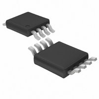
LTC1663IMS8 Linear Technology, LTC1663IMS8 Datasheet - Page 10

LTC1663IMS8
Manufacturer Part Number
LTC1663IMS8
Description
IC DAC 10BIT R-R MICROPWR 8MSOP
Manufacturer
Linear Technology
Datasheet
1.LTC1663CS5TRMPBF.pdf
(12 pages)
Specifications of LTC1663IMS8
Settling Time
30µs
Number Of Bits
10
Data Interface
Serial
Number Of Converters
1
Voltage Supply Source
Single Supply
Power Dissipation (max)
630µW
Operating Temperature
-40°C ~ 85°C
Mounting Type
Surface Mount
Package / Case
8-MSOP, Micro8™, 8-uMAX, 8-uSOP,
Lead Free Status / RoHS Status
Contains lead / RoHS non-compliant
Available stocks
Company
Part Number
Manufacturer
Quantity
Price
Company:
Part Number:
LTC1663IMS8
Manufacturer:
LT
Quantity:
5 321
Company:
Part Number:
LTC1663IMS8
Manufacturer:
LT
Quantity:
10 000
Part Number:
LTC1663IMS8
Manufacturer:
LINEAR/凌特
Quantity:
20 000
Company:
Part Number:
LTC1663IMS8#PBF
Manufacturer:
LINEAR
Quantity:
10
Part Number:
LTC1663IMS8#TR
Manufacturer:
LT/凌特
Quantity:
20 000
Company:
Part Number:
LTC1663IMS8#TRPBF
Manufacturer:
LINEAR
Quantity:
13 257
Part Number:
LTC1663IMS8#TRPBF
Manufacturer:
LINEAR/凌特
Quantity:
20 000
APPLICATIONS INFORMATION
LTC1663
Offset and linearity are defi ned and tested over the region
of the DAC transfer function where no output limiting can
occur.
Internal Reference
In applications where a predictable output is required
that is independent of supply voltage, the LTC1663 has a
user-selectable internal reference. Selecting the internal
reference will set the full-scale output voltage to 2.5V. This
can be useful in applications where the supply voltage is
poorly regulated.
Using the LT
Power Supply for the LTC1663
In applications where the advantages of using the internal
reference are required but the full-scale range needs to
be greater than 2.5V, an external series reference can be
10
Figure 1. Effects of Rail-to-Rail Operation On a DAC Transfer Curve. (a) Overall Transfer Function (b) Effect of Negative
Offset for Codes Near Zero Scale (c) Effect of Positive Full-Scale Error for Input Codes Near Full Scale When V
NEGATIVE
®
OFFSET
1460 Micropower Series Reference as a
VOLTAGE
OUTPUT
0V
INPUT CODE
(b)
VOLTAGE
OUTPUT
0
INPUT CODE
V
REF
512
(a)
= V
CC
used. The LT1460 is ideal for use as a power supply for
the LTC1663 and can provide 3V, 3.3V and 5V full-scale
output voltage ranges. The LT1460 provides accuracy, noise
immunity and extended supply range to the LTC1663 when
the LTC1663 is operated ratiometric to V
parts are available in SOT-23 packages, the PC board space
for this application is extremely small. See Figure 2.
3.9V TO 20V
0.1μF
LTC1663 PIN NUMBERS IN PARENTHESES
REFER TO MSOP PACKAGE
Figure 2. LT1460 As Power Supply for the LTC1663
1023
1
IN
LT1460S3-3
GND
3
V
REF
OUT
INPUT CODE
TO
μP
= V
(c)
2
CC
+
5 (4)
1 (1)
0.01μF
SCL
SDA
LTC1663
3V
GND
V
CC
4 (5)
2 (7)
OUTPUT
VOLTAGE
POSITIVE
FSE
1663 F01
OUT
REF
CC
. Since both
3 (8)
= V
0V ≤ V
CC
OUT
1663 F02
1663fd
≤ 3V


