LTC1663IMS8 Linear Technology, LTC1663IMS8 Datasheet
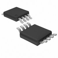
IC DAC 10BIT R-R MICROPWR 8MSOP

LTC1663IMS8

Manufacturer Part Number
LTC1663IMS8
Description
IC DAC 10BIT R-R MICROPWR 8MSOP
Manufacturer
Linear Technology
Datasheet

Specifications of LTC1663IMS8

Settling Time
30µs
Number Of Bits
10
Data Interface
Serial
Number Of Converters
1
Voltage Supply Source
Single Supply
Power Dissipation (max)
630µW
Operating Temperature
-40°C ~ 85°C
Mounting Type
Surface Mount
Package / Case
8-MSOP, Micro8™, 8-uMAX, 8-uSOP,
Lead Free Status / RoHS Status
Contains lead / RoHS non-compliant

Available stocks

Company
Part Number
Manufacturer
Quantity
Price
Part Number:
LTC1663IMS8
Manufacturer:
LT
Quantity:
5 321
Part Number:
LTC1663IMS8
Manufacturer:
LT
Quantity:
10 000
Part Number:
LTC1663IMS8
Manufacturer:
LINEAR/凌特
Quantity:
20 000
Part Number:
LTC1663IMS8#PBF
Manufacturer:
LINEAR
Quantity:
10
Part Number:
LTC1663IMS8#TR
Manufacturer:
LT/凌特
Quantity:
20 000
Part Number:
LTC1663IMS8#TRPBF
Manufacturer:
LINEAR
Quantity:
13 257
Part Number:
LTC1663IMS8#TRPBF
Manufacturer:
LINEAR/凌特
Quantity:
20 000
FEATURES
APPLICATIONS
n
n
n
n
n
n
n
n
n
n
n
n
n
n
n
n
n
n
BLOCK DIAGRAM
PACKAGE
MSOP
ONLY
Micropower 10-Bit DAC in SOT-23
Low Operating Current: 60μA
Ultralow Power Shutdown Mode: 10μA
2-Wire Serial Interface Compatible
with SMBus
Selectable Internal Reference or Ratiometric to
V
Maximum DNL Error: 0.75LSB
8 User Selectable Addresses (MSOP Package)
Single 2.7V to 5.5V Operation
Buffered True Rail-to-Rail Voltage Output
Power-On Reset
0.6V V
Small 5-Lead SOT-23 and 8-Lead MSOP Packages
Digital Calibration
Offset/Gain Adjustment
Industrial Process Control
Automatic Test Equipment
Arbitrary Function Generators
Battery-Powered Data Conversion Products
(6)
(2)
(3)
CC
NOTE: PIN NUMBERS IN PARENTHESES REFER TO THE MSOP PACKAGE
AD0
AD1
AD2
IL
COMMAND
and 1.4V V
LATCH
2-WIRE INTERFACE
SDA
1 (1)
DAC LATCH
10-BIT
INPUT
LATCH
IH
SCL
5 (4)
1.25V
for SDA and SCL
REFERENCE
BANDGAP
REFERENCE
SELECT
4 (5)
V
CC
GND
2 (7)
R
+
R
V
OUT
1663 BD
DESCRIPTION
The LTC
buffered rail-to-rail output voltage capability. It operates
from a single supply with a range of 2.7V to 5.5V. The
reference for the DAC is selectable between the supply
voltage or an internal bandgap reference. Selecting the
internal bandgap reference will set the full-scale output
voltage range to 2.5V. Selecting the supply as the reference
sets the output voltage range to the supply voltage.
The part features a simple 2-wire serial interface compat-
ible with SMBus that allows communication between many
devices. The internal data registers are double buffered to
allow for simultaneous update of several devices at once.
The DAC can be put in low current power-down mode for
use in power conscious systems.
Power-on reset ensures the DAC output is at 0V when
power is initially applied, and all internal registers are
cleared.
For I
L, LT, LTC and LTM are registered trademarks of Linear Technology Corporation. All other
trademarks are the property of their respective owners.
3 (8)
2
C designs, please refer to the LTC1669.
®
Micropower DAC with
1663 is a 10-bit voltage output DAC with true
–1.0
–0.2
–0.4
–0.6
–0.8
1.0
0.8
0.6
0.4
0.2
Differential Nonlinearity (DNL)
0
10-Bit Rail-to-Rail
2-Wire Interface
0
V
T
REF
A
28
= 25°C
= V
156
CC
= 5V
384
CODE
512 640
LTC1663
768 896 1024
1663 TA01
1663fd
1

Related parts for LTC1663IMS8

LTC1663IMS8 Summary of contents

Page 1

... Power-on reset ensures the DAC output when power is initially applied, and all internal registers are cleared. 2 For I C designs, please refer to the LTC1669. L, LT, LTC and LTM are registered trademarks of Linear Technology Corporation. All other trademarks are the property of their respective owners ...

Page 2

... LTC1663C ............................................... 0°C to 70°C + 0.3V) LTC1663I............................................. –40°C to 85° 0.3V) LTC1663E (Note 8) .............................. –40°C to 85°C CC Lead Temperature (Soldering, 10 sec) ................. 300°C ORDER PART NUMBER LTC1663CMS8 SDA 1 LTC1663IMS8 GND 2 LTC1663-8CMS8 V 3 OUT LTC1663-8IMS8 5-LEAD PLASTIC SOT-23 MS8 PART MARKING T JMAX LTEQ ...

Page 3

ELECTRICAL CHARACTERISTICS range, otherwise specifi cations are SYMBOL PARAMETER V Positive Supply Voltage CC I Supply Current CC I Supply Current in Shutdown Mode SD Op Amp DC Performance Short-Circuit Current (Sourcing) Short-Circuit Current (Sinking) Output Impedance ...

Page 4

LTC1663 TIMING CHARACTERISTICS range, otherwise specifi cations are at T SYMBOL PARAMETER t Data Setup Time SU, DAT t Clock Low Period LOW t Clock High Period HIGH t Clock, Data Fall Time f t Clock, Data Rise Time r ...

Page 5

TYPICAL PERFORMANCE CHARACTERISTICS Load Regulation vs Output Current 1 REF 0 1.5V OUT CODE = 512 0 25°C A 0.4 0.2 0 –0.2 SOURCE SINK –0.4 –0.6 –0.8 –1.0 –1.0 ...

Page 6

LTC1663 TIMING DIAGRAM 6 1663fd ...

Page 7

DEFINITIONS Integral Nonlinearity (INL): The deviation from a straight line passing through the endpoints of the DAC transfer curve (Endpoint INL). Because the output cannot go below zero, the linearity is measured between full scale and the lowest code that ...

Page 8

LTC1663 APPLICATIONS INFORMATION Bit (Wr The LTC1663 acknowledges and the master delivers the command byte. The LTC1663 acknowledges and latches the command byte into the command byte input register. The master then delivers the least signifi cant data ...

Page 9

APPLICATIONS INFORMATION Data Bytes Least Signifi cant Data Byte Most Signifi cant Data Byte Don’t care Send Byte ...

Page 10

LTC1663 APPLICATIONS INFORMATION OUTPUT VOLTAGE 0V NEGATIVE INPUT CODE OFFSET (b) Figure 1. Effects of Rail-to-Rail Operation On a DAC Transfer Curve. (a) Overall Transfer Function (b) Effect of Negative Offset for Codes Near Zero Scale (c) Effect of Positive ...

Page 11

... LEAD COPLANARITY (BOTTOM OF LEADS AFTER FORMING) SHALL BE 0.102mm (.004") MAX Information furnished by Linear Technology Corporation is believed to be accurate and reliable. However, no responsibility is assumed for its use. Linear Technology Corporation makes no representa- tion that the interconnection of its circuits as described herein will not infringe on existing patent rights. ...

Page 12

... AD2 GND 0.1μF SCL V CC SDA 8 LTC1663CMS8 CONTROL V OUT AD0 OUTPUT 15 0V ≤ V < V AD1 OUT15 CC AD2 GND 7 1663 TA06 DAC. Output Swings from GND to REF . OUT . 3-Wire Interface 1007 REV D • PRINTED IN USA © LINEAR TECHNOLOGY CORPORATION 2007 1663fd ...

Related keywords