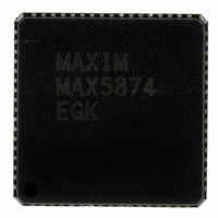
MAX5874EGK+D Maxim Integrated Products, MAX5874EGK+D Datasheet - Page 8

MAX5874EGK+D
Manufacturer Part Number
MAX5874EGK+D
Description
IC DAC 14BIT 200MSPS DUAL 68-QFN
Manufacturer
Maxim Integrated Products
Datasheet
1.MAX5874EGKD.pdf
(16 pages)
Specifications of MAX5874EGK+D
Settling Time
14ns
Number Of Bits
14
Data Interface
Parallel
Number Of Converters
2
Voltage Supply Source
Analog and Digital
Power Dissipation (max)
300mW
Operating Temperature
-40°C ~ 85°C
Mounting Type
Surface Mount
Package / Case
68-QFN Exposed Pad
Lead Free Status / RoHS Status
Lead free / RoHS Compliant
14-Bit, 200Msps, High-Dynamic-Performance,
Dual DAC with CMOS Inputs
8
10, 12, 13, 15,
20, 23, 26, 27,
14, 21, 22, 31,
30, 33, 36, 43
8, 9, 59, 60
_______________________________________________________________________________________
19, 34
PIN
1–7
11
32
16
17
18
24
25
28
29
35
37
38
39
40
41
A3, A2, A1, A0
A6, A5, A4,
DACREF
DV
AV
AV
OUTQN
OUTQP
FSADJ
OUTIN
NAME
REFIO
OUTIP
AV
CLKN
TORB
CLKP
DORI
GND
N.C.
PD
DD3.3
DD3.3
DD1.8
CLK
Data Bits A6–A0. In dual-port mode, data is directed to the Q-DAC. In single-port mode, data bits
are not used. Connect bits A6–A0 to GND in single-port mode.
No Connection. Leave floating or connect to GND.
Converter Ground
Digital Supply Voltage. Accepts a 3.135V to 3.465V supply voltage range. Bypass with a 0.1µF
capacitor to GND.
Analog Supply Voltage. Accepts a 3.135V to 3.465V supply voltage range. Bypass each pin with
a 0.1µF capacitor to GND.
Reference I/O. Output of the internal 1.2V precision bandgap reference. Bypass with a 1µF
capacitor to GND. REFIO can be driven with an external reference source. See Table1.
Full-Scale Adjust Input. This input sets the full-scale output current of the DAC. For a 20mA full-
scale output current, connect a 2kΩ resistor between FSADJ and DACREF. See Table1.
Current-Set Resistor Return Path. For a 20mA full-scale output current, connect a 2kΩ resistor
between FSADJ and DACREF. Internally connected to GND. Do not use as an external ground
connection.
Analog Supply Voltage. Accepts a 1.71V to 1.89V supply voltage range. Bypass each pin with a
0.1µF capacitor to GND.
Complementary Q-DAC Output. Negative terminal for current output.
Q-DAC Output. Positive terminal for current output.
Complementary I-DAC Output. Negative terminal for current output.
I-DAC Output. Positive terminal for current output.
Clock Supply Voltage. Accepts a 3.135V to 3.465V supply voltage range. Bypass with a 0.1µF
capacitor to GND.
Complementary Converter Clock Input. Negative input terminal for differential converter clock.
Internally biased to AV
Converter Clock Input. Positive input terminal for differential converter clock. Internally biased to
AV
Two’s-Complement/Binary Select Input. Set TORB to a CMOS-logic-high level to indicate a two’s-
complement input format. Set TORB to a CMOS-logic-low level to indicate a binary input format.
TORB has an internal pulldown resistor.
Power-Down Input. Set PD to a CMOS-logic-high level to force the DAC into power-down mode.
Set PD to a CMOS-logic-low level for normal operation. PD has an internal pulldown resistor.
Dual (Parallel)/Single (Interleaved) Port Select Input. Set DORI high to configure as a dual-port
DAC. Set DORI low to configure as a single-port interleaved DAC. DORI has an internal pulldown
resistor.
CLK
/ 2.
CLK
/ 2.
FUNCTION
Pin Description


