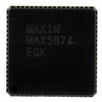
MAX5874EGK+D Maxim Integrated Products, MAX5874EGK+D Datasheet - Page 14

MAX5874EGK+D
Manufacturer Part Number
MAX5874EGK+D
Description
IC DAC 14BIT 200MSPS DUAL 68-QFN
Manufacturer
Maxim Integrated Products
Datasheet
1.MAX5874EGKD.pdf
(16 pages)
Specifications of MAX5874EGK+D
Settling Time
14ns
Number Of Bits
14
Data Interface
Parallel
Number Of Converters
2
Voltage Supply Source
Analog and Digital
Power Dissipation (max)
300mW
Operating Temperature
-40°C ~ 85°C
Mounting Type
Surface Mount
Package / Case
68-QFN Exposed Pad
Lead Free Status / RoHS Status
Lead free / RoHS Compliant
14-Bit, 200Msps, High-Dynamic-Performance,
Dual DAC with CMOS Inputs
Figure 7. Differential Output Configuration
optimizing the DAC’s dynamic performance. Keep digi-
tal signal paths short and run lengths matched to avoid
propagation delay and data skew mismatches.
The MAX5874 requires five separate power-supply
inputs for analog (AV
(DV
Decouple each AV
a separate 0.1µF capacitor as close to the device as
possible with the shortest possible connection to the
ground plane (Figure 8). Minimize the analog and digi-
tal load capacitances for optimized operation.
Decouple all three power-supply voltages at the point
they enter the PCB with tantalum or electrolytic capaci-
tors. Ferrite beads with additional decoupling capaci-
tors forming a pi-network could also improve
performance.
The analog and digital power-supply inputs AV
AV
voltage range. The analog and digital power-supply
inputs AV
supply voltage range.
The MAX5874 is packaged in a 68-pin QFN-EP pack-
age, providing greater design flexibility and optimized
DAC AC performance. The EP enables the use of nec-
essary grounding techniques to ensure highest perfor-
mance operation. Thermal efficiency is not the key
factor, since the MAX5874 features low-power opera-
tion. The exposed pad ensures a solid ground connec-
tion between the DAC and the PCB’s ground layer.
14
DATA13–DATA0
CLK
DD1.8
______________________________________________________________________________________
, and DV
14
and DV
DD1.8
DD3.3
and DV
MAX5874
DD3.3
DD
GND
, DV
allow a 3.135V to 3.465V supply
), and clock (AV
DD1.8
DD1.8
DD
, and AV
OUTIP/OUTQP
OUTIN/OUTQN
allow a 1.71V to 1.89V
and AV
CLK
DD3.3
CLK
input pin with
25Ω
50Ω
25Ω
) circuitry.
), digital
DD3.3
OUTP
OUTN
,
The data converter die attaches to an EP lead frame
with the back of this frame exposed at the package
bottom surface, facing the PCB side of the package.
This allows for a solid attachment of the package to the
PCB with standard infrared (IR) reflow soldering tech-
niques. A specially created land pattern on the PCB,
matching the size of the EP (6mm x 6mm), ensures the
proper attachment and grounding of the DAC. Refer to
the MAX5874 EV kit data sheet. Designing vias into the
land area and implementing large ground planes in the
PCB design allow for the highest performance opera-
tion of the DAC. Use an array of at least 4 x 4 vias
(≤ 0.3mm diameter per via hole and 1.2mm pitch
between via holes) for this 68-pin QFN-EP package.
Connect the MAX5874 exposed paddle to GND. Vias
connect the land pattern to internal or external copper
planes. Use as many vias as possible to the ground
plane to minimize inductance.
Figure 8. Recommended Power-Supply Decoupling and
Bypassing Circuitry
*BYPASS EACH POWER-SUPPLY PIN INDIVIDUALLY.
BYPASSING—DAC LEVEL
DATA13–DATA0
14
AV
DV
DD1.8
DD1.8
0.1µF
0.1µF
DV
AV
MAX5874
DD3.3
DD3.3
0.1µF
0.1µF
AV
CLK
OUTIP/OUTQP
OUTIN/OUTQN
0.1µF


