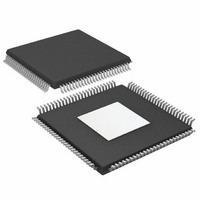
AD9788BSVZ Analog Devices Inc, AD9788BSVZ Datasheet - Page 30

AD9788BSVZ
Manufacturer Part Number
AD9788BSVZ
Description
IC DAC 16BIT 800MSPS 100TQFP
Manufacturer
Analog Devices Inc
Series
TxDAC®r
Datasheet
1.AD9785BSVZ.pdf
(64 pages)
Specifications of AD9788BSVZ
Data Interface
Serial
Design Resources
Powering the AD9788 Using ADP2105 for Increased Efficiency (CN0141)
Number Of Bits
16
Number Of Converters
2
Voltage Supply Source
Analog and Digital
Power Dissipation (max)
450mW
Operating Temperature
-40°C ~ 85°C
Mounting Type
Surface Mount
Package / Case
100-TQFP Exposed Pad, 100-eTQFP, 100-HTQFP, 100-VQFP
Resolution (bits)
16bit
Sampling Rate
800MSPS
Input Channel Type
Parallel
Digital Ic Case Style
QFP
No. Of Pins
100
Operating Temperature Range
-40°C To +85°C
Number Of Channels
2
Resolution
16b
Interface Type
Parallel
Single Supply Voltage (typ)
3.3V
Dual Supply Voltage (typ)
Not RequiredV
Settling Time
0.02us
Architecture
Interpolation Filter
Power Supply Requirement
Analog and Digital
Output Type
Current
Integral Nonlinearity Error
±3.7LSB
Single Supply Voltage (min)
3.13V
Single Supply Voltage (max)
3.47V
Dual Supply Voltage (min)
Not RequiredV
Dual Supply Voltage (max)
Not RequiredV
Operating Temp Range
-40C to 85C
Operating Temperature Classification
Industrial
Mounting
Surface Mount
Pin Count
100
Package Type
TQFP EP
Lead Free Status / RoHS Status
Lead free / RoHS Compliant
For Use With
AD9788-EBZ - BOARD EVAL FOR AD9788
Settling Time
-
Lead Free Status / Rohs Status
Compliant
Available stocks
Company
Part Number
Manufacturer
Quantity
Price
Company:
Part Number:
AD9788BSVZ
Manufacturer:
AD
Quantity:
490
Company:
Part Number:
AD9788BSVZ
Manufacturer:
Analog Devices Inc
Quantity:
10 000
Part Number:
AD9788BSVZ
Manufacturer:
ADI/亚德诺
Quantity:
20 000
Company:
Part Number:
AD9788BSVZRL
Manufacturer:
Analog Devices Inc
Quantity:
10 000
Part Number:
AD9788BSVZRL
Manufacturer:
ADI/亚德诺
Quantity:
20 000
AD9785/AD9787/AD9788
The Auxiliary DAC 1 control register comprises two bytes located at Address 0x06. These bits are routed directly to the periphery of the
digital logic. No digital functionality within the main digital block is required.
Table 16. Auxiliary DAC 1 Control Register
Address
0x06
The Q DAC control register comprises two bytes located at Address 0x07. These bits are routed directly to the periphery of the digital
logic. No digital functionality within the main digital block is required.
Table 17. Q DAC Control Register
Address
0x07
The Auxiliary DAC 2 control register comprises two bytes located at Address 0x08. These bits are routed directly to the periphery of the
digital logic. No digital functionality within the main digital block is required.
Table 18. Auxiliary DAC 2 Control Register
Address
0x08
Bit
[15]
[14]
[13]
[12:10]
[9:0]
Bit
[15]
[14]
[13:10]
[9:0]
Bit
[15]
[14]
[13]
[12:10]
[9:0]
Name
Auxiliary DAC 1 sign
Auxiliary DAC 1
current direction
Auxiliary DAC 1
power-down
Reserved
Auxiliary DAC 1 data
Name
Q DAC sleep
Q DAC power-down
Reserved
Q DAC gain adjustment
Auxiliary DAC 2 sign
Auxiliary DAC 2
current direction
Auxiliary DAC 2
power-down
Reserved
Auxiliary DAC 2 data
Name
0: Default. If the Auxiliary DAC 1 sign bit is cleared, the Aux DAC 1 sign is positive.
Pin 90 is the active pin.
1: If the Auxiliary DAC 1 sign bit is set, the Aux DAC 1 sign is negative. Pin 89 is the
active pin.
0: Default. If the Auxiliary DAC 1 current direction bit is cleared, the Aux DAC 1 sources
current.
1: If the Auxiliary DAC 1 current direction bit is set, the Aux DAC 1 sinks current.
0: Default. If the Auxiliary DAC 1 power-down bit is cleared, the Aux DAC 1 is active.
1: If the Auxiliary DAC 1 power-down bit is set, the Aux DAC 1 is inactive and enters a
low power state.
Reserved for future use.
These bits are the Auxiliary DAC 1 gain adjustment bits.
Description
Description
0: Default. If the Q DAC sleep bit is cleared, the Q DAC is active.
1: If the Q DAC sleep bit is set, the Q DAC is inactive and enters a low power state.
0: Default. If the Q DAC power-down bit is cleared, the Q DAC is active.
1: If the Q DAC power-down bit is set, the Q DAC is inactive and enters a low power state.
Reserved for future use.
These bits are the Q DAC gain adjustment bits.
Description
0: Default. If the Auxiliary DAC 2 sign bit is cleared, the Aux DAC 2 sign is positive.
Pin 86 is the active pin.
1: If the Auxiliary DAC 2 sign bit is set, the Aux DAC 2 sign is negative. Pin 87 is the
active pin.
0: Default. If the Auxiliary DAC 2 current direction bit is cleared, the Aux DAC 2 sources
current.
1: If the Auxiliary DAC 2 current direction bit is set, the Aux DAC 2 sinks current.
0: Default. If the Auxiliary DAC 2 power-down bit is cleared, the Aux DAC 2 is active.
1: If the Auxiliary DAC 2 power-down bit is set, the Aux DAC 2 is inactive and enters
a low power state.
Reserved for future use.
These bits are the Auxiliary DAC 2 gain adjustment bits.
Rev. A | Page 30 of 64


