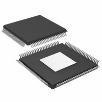
AD9788BSVZ Analog Devices Inc, AD9788BSVZ Datasheet - Page 22

AD9788BSVZ
Manufacturer Part Number
AD9788BSVZ
Description
IC DAC 16BIT 800MSPS 100TQFP
Manufacturer
Analog Devices Inc
Series
TxDAC®r
Datasheet
1.AD9785BSVZ.pdf
(64 pages)
Specifications of AD9788BSVZ
Data Interface
Serial
Design Resources
Powering the AD9788 Using ADP2105 for Increased Efficiency (CN0141)
Number Of Bits
16
Number Of Converters
2
Voltage Supply Source
Analog and Digital
Power Dissipation (max)
450mW
Operating Temperature
-40°C ~ 85°C
Mounting Type
Surface Mount
Package / Case
100-TQFP Exposed Pad, 100-eTQFP, 100-HTQFP, 100-VQFP
Resolution (bits)
16bit
Sampling Rate
800MSPS
Input Channel Type
Parallel
Digital Ic Case Style
QFP
No. Of Pins
100
Operating Temperature Range
-40°C To +85°C
Number Of Channels
2
Resolution
16b
Interface Type
Parallel
Single Supply Voltage (typ)
3.3V
Dual Supply Voltage (typ)
Not RequiredV
Settling Time
0.02us
Architecture
Interpolation Filter
Power Supply Requirement
Analog and Digital
Output Type
Current
Integral Nonlinearity Error
±3.7LSB
Single Supply Voltage (min)
3.13V
Single Supply Voltage (max)
3.47V
Dual Supply Voltage (min)
Not RequiredV
Dual Supply Voltage (max)
Not RequiredV
Operating Temp Range
-40C to 85C
Operating Temperature Classification
Industrial
Mounting
Surface Mount
Pin Count
100
Package Type
TQFP EP
Lead Free Status / RoHS Status
Lead free / RoHS Compliant
For Use With
AD9788-EBZ - BOARD EVAL FOR AD9788
Settling Time
-
Lead Free Status / Rohs Status
Compliant
Available stocks
Company
Part Number
Manufacturer
Quantity
Price
Company:
Part Number:
AD9788BSVZ
Manufacturer:
AD
Quantity:
490
Company:
Part Number:
AD9788BSVZ
Manufacturer:
Analog Devices Inc
Quantity:
10 000
Part Number:
AD9788BSVZ
Manufacturer:
ADI/亚德诺
Quantity:
20 000
Company:
Part Number:
AD9788BSVZRL
Manufacturer:
Analog Devices Inc
Quantity:
10 000
Part Number:
AD9788BSVZRL
Manufacturer:
ADI/亚德诺
Quantity:
20 000
AD9785/AD9787/AD9788
There are two phases to a communication cycle with the
AD9785/AD9787/AD9788. Phase 1 is the instruction cycle,
which is the writing of an instruction byte into the AD9785/
AD9787/AD9788, coincident with the first eight SCLK rising
edges. The instruction byte provides the AD9785/AD9787/
AD9788 serial port controller with information regarding the
data transfer cycle, which is Phase 2 of the communication
cycle. The instruction byte defines whether the upcoming data
transfer is read or write and the serial address of the register
being accessed.
The first eight SCLK rising edges of each communication cycle
are used to write the instruction byte into the AD9785/AD9787/
AD9788. The remaining SCLK edges are for Phase 2 of the
communication cycle. Phase 2 is the actual data transfer
between the AD9785/AD9787/AD9788 and the system
controller. The number of bytes transferred during Phase 2 of
the communication cycle is a function of the register being
accessed.
For example, when accessing the frequency tuning word (FTW)
register, which is four bytes wide, Phase 2 requires that four
bytes be transferred. If accessing the amplitude scale factor (ASF)
register, which is three bytes wide, Phase 2 requires that three
bytes be transferred. After transferring all data bytes per the
instruction byte, the communication cycle is completed.
At the completion of any communication cycle, the AD9785/
AD9787/AD9788 serial port controller expects the next eight
rising SCLK edges to be the instruction byte of the next
communication cycle.
All data input is registered on the rising edge of SCLK. All data
is driven out of the AD9785/AD9787/AD9788 on the falling
edge of SCLK.
Rev. A | Page 22 of 64
Figure 43 through Figure 46 are useful in understanding the
general operation of the AD9785/AD9787/AD9788 serial port.
SPI_SDIO
SPI_SDIO
SPI_SDIO
SPI_SDIO
SPI_CSB
SPI_SDO
SPI_CSB
SPI_SDO
SPI_CSB
SPI_CSB
SPI_SDO
SCLK
SCLK
SCLK
SCLK
Figure 43. Serial Register Interface Timing, MSB First
Figure 46. SPI Register Read Timing Instruction Byte
Figure 44. Serial Register Interface Timing, LSB First
R/W N1 N0
A0
INSTRUCTION CYCLE
INSTRUCTION BIT 7
INSTRUCTION CYCLE
A1 A2
t
t
DS
DS
Figure 45. SPI Register Write Timing
DATA BIT n
A4 A3
A3 A4
t
PWH
t
t
DV
DH
t
A2 A1
N0 N1 R/W D0
SCLK
t
PWL
INSTRUCTION BIT 6
A0 D7 D6
DATA BIT n–1
D0
D7 D6
0
0
DATA TRANSFER CYCLE
DATA TRANSFER CYCLE
D1
D1
N
N
0
0
D5
D5
D2
D2
N
N
0
0
D3
D4
D4
D3
0
N
0
N
D2
D5
D5
D2
0
0
N
N
D6
D1
D1
D6
0
N
0
N
D0
D7
D7
D0
0
0
N
N


