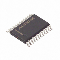
MAX5590BEUG+ Maxim Integrated Products, MAX5590BEUG+ Datasheet - Page 5

MAX5590BEUG+
Manufacturer Part Number
MAX5590BEUG+
Description
IC DAC 12BIT OCTAL BUFF 24-TSSOP
Manufacturer
Maxim Integrated Products
Datasheet
1.MAX5590BEUG.pdf
(33 pages)
Specifications of MAX5590BEUG+
Settling Time
3µs
Number Of Bits
12
Data Interface
Serial
Number Of Converters
8
Voltage Supply Source
Analog and Digital
Operating Temperature
-40°C ~ 85°C
Mounting Type
Surface Mount
Package / Case
24-TSSOP
Resolution
12 bit
Interface Type
Serial (SPI)
Supply Voltage (max)
5.25 V
Supply Voltage (min)
2.7 V
Maximum Operating Temperature
+ 85 C
Mounting Style
SMD/SMT
Minimum Operating Temperature
- 40 C
Supply Current
3.2 mA
Voltage Reference
External
Lead Free Status / RoHS Status
Lead free / RoHS Compliant
Power Dissipation (max)
-
Lead Free Status / Rohs Status
Lead free / RoHS Compliant
ELECTRICAL CHARACTERISTICS (continued)
(AV
AV
(Note 1)
Note 1: For the force-sense versions, FB_ is connected to its respective OUT_. V OUT (max) = V REF / 2, unless otherwise noted.
Note 2: Linearity guaranteed from decimal code 40 to code 4095 for the MAX5590B/MAX5591B (12-bit, B-grade), code 10 to code
Note 3: Represents the functional range. The linearity is guaranteed at V REF = 2.5V (for AV DD from 2.7V to 5.25V), and V REF =
Note 4: DC crosstalk is measured as follows: outputs of DACA–DACH are set to full scale and the output of DACH is measured.
Note 5: Guaranteed by design.
Note 6: The reference -3dB bandwidth is measured with a 0.1V P-P sine wave on V REF and with full-scale input code.
POWER REQUIREMENTS
Analog Supply Voltage
Range
Digital Supply Voltage
Range
Operating Supply
Current
Shutdown Supply
Current
DD
DD
PARAMETER
= 4.5V to 5.25V), R
= 2.7V to 5.25V, DV
1023 for the MAX5592/MAX5593 (10-bit), and code 3 to code 255 for the MAX5594/MAX5595 (8-bit).
4.096V (for AV DD = 4.5V to 5.25V). See the Typical Operating Characteristics section for linearity at other voltages.
While keeping DACH unchanged, the outputs of DACA–DACG are transitioned to zero scale and the ∆V OUT of DACH is
measured.
Buffered, Fast-Settling, Octal, 12/10/8-Bit,
_______________________________________________________________________________________
L
DD
= 10kΩ, C
I
I
D V D D ( S H D N )
AV D D ( S H D N )
SYMBOL
= 1.8V to AV
DV
I
I
AV
DVDD
AVDD
+
+
DD
DD
L
= 100pF, T
SLOW mode, all digital inputs
at DGND or DV
V
FAST mode, all digital inputs
at DGND or DV
V
No clocks, all digital inputs at DGND or DV
DACs in shutdown mode
REF
REF
DD
, V
= 4.096V
= 4.096V
AGND
A
= T
= 0V, V
MIN
DD
DD
, no load,
, no load,
to T
CONDITIONS
DGND
MAX
, unless otherwise noted. Typical values are at T
= 0V, V
Unity gain
Force sense
Unity gain
Force sense
Voltage-Output DACs
REF
= 2.5V (for AV
DD
, all
DD
= 2.7V to 5.25V), V
MIN
2.70
1.8
TYP
1.5
2.4
2.5
3.4
0.5
A
REF
AV
MAX
5.25
= +25°C.)
3.2
4.8
8
8
1
DD
= 4.096V (for
UNITS
mA
µA
V
V
5


