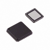
AD9717BCPZ Analog Devices Inc, AD9717BCPZ Datasheet - Page 45

AD9717BCPZ
Manufacturer Part Number
AD9717BCPZ
Description
IC DAC DUAL 14BIT LO PWR 40LFCSP
Manufacturer
Analog Devices Inc
Series
TxDAC®r
Datasheet
1.AD9717BCPZ.pdf
(80 pages)
Specifications of AD9717BCPZ
Data Interface
Serial
Number Of Bits
14
Number Of Converters
2
Voltage Supply Source
Analog and Digital
Power Dissipation (max)
86mW
Operating Temperature
-40°C ~ 85°C
Mounting Type
Surface Mount
Package / Case
40-LFCSP
Resolution (bits)
14bit
Sampling Rate
125MSPS
Input Channel Type
Parallel, Serial
Supply Current
11mA
Digital Ic Case Style
CSP
No. Of Pins
40
Lead Free Status / RoHS Status
Lead free / RoHS Compliant
Settling Time
-
Lead Free Status / RoHS Status
Lead free / RoHS Compliant, Lead free / RoHS Compliant
Available stocks
Company
Part Number
Manufacturer
Quantity
Price
Company:
Part Number:
AD9717BCPZ
Manufacturer:
ADI
Quantity:
172
Part Number:
AD9717BCPZ
Manufacturer:
ADI/亚德诺
Quantity:
20 000
SELF-CALIBRATION
The AD9714/AD9715/AD9716/AD9717 have a self-calibration
feature that improves the DNL of the device. Performing a self-
calibration on the device improves device performance in low
frequency applications. The device performance in applications
where the analog output frequencies are above 5 MHz are generally
influenced more by dynamic device behavior than by DNL and,
in these cases, self-calibration is unlikely to provide much benefit.
The calibration clock frequency is equal to the DAC clock
divided by the division factor chosen by the DIVSEL value. Each
calibration clock cycle is between 32 and 2048 DAC input clock
cycles, depending on the value of DIVSEL[2:0] (Register 0x0E,
Bits[2:0]). The frequency of the calibration clock should be
between 0.5 MHz and 4 MHz for reliable calibrations. Best
results are obtained by setting DIVSEL[2:0] (Register 0x0E,
Bits[2:0]) to produce a calibration clock frequency between
these values. Separate self-calibration hardware is included
for each DAC. The DACs can be self-calibrated individually or
simultaneously.
To perform a device self-calibration, the following procedure
can be used:
1.
2.
3.
4.
5.
6.
7.
Write 0x00 to Register 0x12. This ensures that the
UNCALI and UNCALQ bits are reset.
Set up a calibration clock between 0.5 MHz and 4 MHz
using DIVSEL[2:0], and then enable the calibration clock
by setting the CALCLK bit (Register 0x0E, Bit 3).
Select the DAC(s) to self-calibrate by setting either Bit 4
(CALSELI) for the I DAC and/or Bit 5 (CALSELQ) for the
Q DAC in Register 0x0E. Note that each DAC contains
independent calibration hardware so that they can be
calibrated simultaneously.
Start self-calibration by setting the CALEN bit (Register 0x12,
Bit 4). Wait approximately 300 calibration clock cycles.
Check if the self-calibration has completed by reading
the CALSTATI bit (Bit 6) and CALSTATQ bit (Bit 7) in
Register 0x0F. Logic 1 indicates that the calibration has
completed.
When the self-calibration has completed, write 0x00 to
Register 0x12.
Disable the calibration clock by clearing the CALCLK bit
(Register 0x0E, Bit 3).
Rev. A | Page 45 of 80
The AD9714/AD9715/AD9716/AD9717 allow reading and
writing of the calibration coefficients. There are 32 coefficients
in total. The read/write feature of the coefficients can be useful
for improving the results of the self-calibration routine by
averaging the results of several self-calibration cycles and
loading the averaged results back into the device.
To read the calibration coefficients, use the following steps:
1.
2.
3.
4.
5.
6.
To write the calibration coefficients to the device, use the
following steps:
1.
2.
3.
4.
5.
6.
7.
Select which DAC core to read by setting either Bit 4
(CALSELI) for the I DAC or Bit 5 (CALSELQ) for the
Q DAC in Register 0x0E. Write the address of the first
coefficient (0x01) to Register 0x10.
Set the SMEMRD bit (Register 0x12, Bit 2) by writing 0x04
to Register 0x12.
Read the 6-bit value of the first coefficient by reading the
contents of Register 0x11.
Clear the SMEMRD bit by writing 0x00 to Register 0x12.
Repeat Step 2 through Step 4 for each of the remaining 31
coefficients by incrementing the address by 1 for each read.
Deselect the DAC core by clearing either Bit 4 (CALSELI)
for the I DAC or Bit 5 (CALSELQ) for the Q DAC in
Register 0x0E.
Select which DAC core to write to by setting either Bit 4
(CALSELI) for the I DAC or Bit 5 (CALSELQ) for the Q
DAC in Register 0x0E.
Set the SMEMWR bit (Register 0x12, Bit 3) by writing 0x08
to Register 0x12.
Write the address of the first coefficient (0x01) to
Register 0x10.
Write the value of the first coefficient to Register 0x11.
Repeat Step 2 through Step 4 for each of the remaining 31
coefficients by incrementing the address by one for each
write.
Clear the SMEMWR bit by writing 0x00 to Register 0x12.
Deselect the DAC core by clearing either Bit 4 (CALSELI)
for the I DAC or Bit 5 (CALSELQ) for the Q DAC in
Register 0x0E.
AD9714/AD9715/AD9716/AD9717


