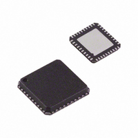
AD9717BCPZ Analog Devices Inc, AD9717BCPZ Datasheet - Page 12

AD9717BCPZ
Manufacturer Part Number
AD9717BCPZ
Description
IC DAC DUAL 14BIT LO PWR 40LFCSP
Manufacturer
Analog Devices Inc
Series
TxDAC®r
Datasheet
1.AD9717BCPZ.pdf
(80 pages)
Specifications of AD9717BCPZ
Data Interface
Serial
Number Of Bits
14
Number Of Converters
2
Voltage Supply Source
Analog and Digital
Power Dissipation (max)
86mW
Operating Temperature
-40°C ~ 85°C
Mounting Type
Surface Mount
Package / Case
40-LFCSP
Resolution (bits)
14bit
Sampling Rate
125MSPS
Input Channel Type
Parallel, Serial
Supply Current
11mA
Digital Ic Case Style
CSP
No. Of Pins
40
Lead Free Status / RoHS Status
Lead free / RoHS Compliant
Settling Time
-
Lead Free Status / RoHS Status
Lead free / RoHS Compliant, Lead free / RoHS Compliant
Available stocks
Company
Part Number
Manufacturer
Quantity
Price
Company:
Part Number:
AD9717BCPZ
Manufacturer:
ADI
Quantity:
172
Part Number:
AD9717BCPZ
Manufacturer:
ADI/亚德诺
Quantity:
20 000
AD9714/AD9715/AD9716/AD9717
Table 8. AD9715 Pin Function Descriptions
Pin No.
1 to 4
5
6
7
8 to 10
11
12 to 15
16
17
18
19
20
21
22
23
24
25
26
27
28
29
30
Mnemonic
DB[7:4]
DVDDIO
DVSS
DVDD
DB[3:1]
DB0 (LSB)
NC
DCLKIO
CVDD
CLKIN
CVSS
CMLQ
RLQN
QOUTN
QOUTP
RLQP
AVSS
AVDD
RLIP
IOUTP
IOUTN
RLIN
Description
Digital Inputs.
Digital I/O Supply Voltage (1.8 V to 3.3 V Nominal).
Digital Common.
Digital Core Supply Voltage (1.8 V). Strap DVDD to DVDDIO at 1.8 V. If DVDDIO > 1.8 V, bypass DVDD with a
1.0 μF capacitor; however, do not otherwise connect it. The LDO should not drive external loads.
Digital Inputs.
Digital Input (LSB).
No Connect. These pins are not connected to the chip.
Data Input/Output Clock. Clock used to qualify input data.
Sampling Clock Supply Voltage (1.8 V to 3.3 V). CVDD must be ≥ DVDD.
LVCMOS Sampling Clock Input.
Sampling Clock Supply Voltage Common.
Q DAC Output Common-Mode Level. When the internal on chip (QR
the on-chip QR
(QR
resistor (see the Using the Internal Termination Resistors section). The recommended value for this external
resistor is 0 Ω.
Load Resistor (500 Ω) to the CMLQ Pin. For the internal load resistor to be used, this pin should be tied to
QOUTN externally.
Complementary Q DAC Current Output. Full-scale current is sourced when all data bits are 0s.
Q DAC Current Output. Full-scale current is sourced when all data bits are 1s.
Load Resistor (500 Ω) to the CMLQ Pin. For the internal load resistor to be used, this pin should be tied to
QOUTP externally.
Analog Common.
Analog Supply Voltage (1.8 V to 3.3 V).
Load Resistor (500 Ω) to the CMLI Pin. For the internal load resistor to be used, this pin should be tied to
IOUTP externally.
I DAC Current Output. Full-scale current is sourced when all data bits are 1s.
Complementary I DAC Current Output. Full-scale current is sourced when all data bits are 0s.
Load Resistor (500 Ω) to the CMLI Pin. For the internal load resistor to be used, this pin should be tied to
IOUTN externally.
CML
) is disabled, this pin is the common-mode load for Q DAC and must be connected to AVSS through a
CML
NOTES
1. NC = NO CONNECT
2. THE EXPOSED PAD IS CONNECTED TO AVSS AND
DVDDIO
DVDD
DVSS
SHOULD BE SOLDERED TO THE GROUND PLANE.
EXPOSED METAL AT PACKAGE CORNERS IS
CONNECTED TO THIS PAD.
resistor. It is recommended to leave this pin unconnected. When the internal on chip
DB7
DB6
DB5
DB4
DB3
DB2
DB1
10
Figure 3. AD9715 Pin Configuration
1
2
3
4
5
6
7
8
9
Rev. A | Page 12 of 80
PIN 1
INDICATOR
(Not to Scale)
AD9715
TOP VIEW
30 RLIN
29 IOUTN
28 IOUTP
27 RLIP
26 AVDD
25 AVSS
24 RLQP
23 QOUTP
22 QOUTN
21 RLQN
CML
) is enabled, this pin is connected to


