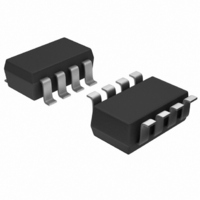
AD5273BRJ100-R2 Analog Devices Inc, AD5273BRJ100-R2 Datasheet - Page 7

AD5273BRJ100-R2
Manufacturer Part Number
AD5273BRJ100-R2
Description
IC DGTL POT 100K 64POS SOT23-8
Manufacturer
Analog Devices Inc
Datasheet
1.AD5273BRJZ10-R7.pdf
(24 pages)
Specifications of AD5273BRJ100-R2
Rohs Status
RoHS non-compliant
Taps
64
Resistance (ohms)
100K
Number Of Circuits
1
Temperature Coefficient
300 ppm/°C Typical
Memory Type
Non-Volatile
Interface
I²C, 2-Wire Serial
Voltage - Supply
2.7 V ~ 5.5 V
Operating Temperature
-40°C ~ 105°C
Mounting Type
Surface Mount
Package / Case
SOT-23-8
Resistance In Ohms
100K
Number Of Elements
1
# Of Taps
64
Resistance (max)
100KOhm
Power Supply Requirement
Single
Interface Type
Serial (2-Wire/I2C)
Single Supply Voltage (typ)
5V
Dual Supply Voltage (typ)
Not RequiredV
Single Supply Voltage (min)
2.7V
Single Supply Voltage (max)
5.5V
Dual Supply Voltage (min)
Not RequiredV
Dual Supply Voltage (max)
Not RequiredV
Operating Temp Range
-40C to 105C
Operating Temperature Classification
Industrial
Mounting
Surface Mount
Pin Count
8
For Use With
AD5273EVAL - BOARD EVAL FOR AD5273
Lead Free Status / RoHS Status
Not Compliant
Other names
AD5273BRJ100-R2TR
PIN CONFIGURATION AND FUNCTION DESCRIPTIONS
Table 3. Pin Function Descriptions
Pin No.
1
2
3
4
5
6
7
8
W
B
A
Mnemonic
V
GND
SCL
SDA
AD0
DD
Description
Wiper Terminal W. GND ≤ V
Positive Power Supply. Specified for non-OTP operation from 2.7 V to 5.5 V. For OTP programming, V
must be set within the window of 5 V to 5.5 V for the 1 kΩ (DD8) and 10 kΩ (DD9) options, or within the
window of 4.75 V to 5.25 V for the 50 kΩ (DYG) and 100 kΩ (DYH) options, and be capable of sourcing 100 mA.
Common Ground.
Serial Clock Input. Requires a pull-up resistor. If it is driven directly from a logic controller without the pull-up
resistor, ensure that the V
Serial Data Input/Output. Requires a pull-up resistor. If it is driven directly from a logic controller without the
pull-up resistor, ensure that the V
I
Resistor Terminal B. GND ≤ V
Resistor Terminal A. GND ≤ V
2
C Device Address Bit. Allows a maximum of two AD5273 devices to be addressed.
IH
GND
SCL
V
W
minimum is 0.7 × V
DD
W
Figure 2. Pin Configuration
B
A
≤ V
≤ V
≤ V
1
2
3
4
Rev. H | Page 7 of 24
DD
DD
(Not to Scale)
IH
DD
.
AD5273
TOP VIEW
minimum is 0.7 × V
.
.
8
7
6
5
DD
A
B
AD0
SDA
.
DD
.
AD5273
DD_OTP


