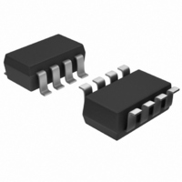
AD5273BRJ100-R2 Analog Devices Inc, AD5273BRJ100-R2 Datasheet - Page 16

AD5273BRJ100-R2
Manufacturer Part Number
AD5273BRJ100-R2
Description
IC DGTL POT 100K 64POS SOT23-8
Manufacturer
Analog Devices Inc
Datasheet
1.AD5273BRJZ10-R7.pdf
(24 pages)
Specifications of AD5273BRJ100-R2
Rohs Status
RoHS non-compliant
Taps
64
Resistance (ohms)
100K
Number Of Circuits
1
Temperature Coefficient
300 ppm/°C Typical
Memory Type
Non-Volatile
Interface
I²C, 2-Wire Serial
Voltage - Supply
2.7 V ~ 5.5 V
Operating Temperature
-40°C ~ 105°C
Mounting Type
Surface Mount
Package / Case
SOT-23-8
Resistance In Ohms
100K
Number Of Elements
1
# Of Taps
64
Resistance (max)
100KOhm
Power Supply Requirement
Single
Interface Type
Serial (2-Wire/I2C)
Single Supply Voltage (typ)
5V
Dual Supply Voltage (typ)
Not RequiredV
Single Supply Voltage (min)
2.7V
Single Supply Voltage (max)
5.5V
Dual Supply Voltage (min)
Not RequiredV
Dual Supply Voltage (max)
Not RequiredV
Operating Temp Range
-40C to 105C
Operating Temperature Classification
Industrial
Mounting
Surface Mount
Pin Count
8
For Use With
AD5273EVAL - BOARD EVAL FOR AD5273
Lead Free Status / RoHS Status
Not Compliant
Other names
AD5273BRJ100-R2TR
AD5273
CONTROLLING THE AD5273
To control the AD5273, users can program the device with
either computer software or with external I
SOFTWARE PROGRAMMING
Because of the OTP feature, users can program the AD5273 in
the factory before shipping it to end users. Therefore, Analog
Devices offers device programming software that can be imple-
mented in the factory on computers running Windows NT,
Windows 2000, and Windows XP platforms. The software,
which can be downloaded from the AD5273 product page at
www.analog.com, is an executable file that does not require any
programming languages or user programming skills. Figure 39
shows the software interface.
Write
The AD5273 starts at midscale after power-up prior to any OTP
programming. To increment or decrement the resistance, move
the scrollbar on the left. Once the desired setting is found, click
Program Permanent to lock the setting permanently. To write
any specific values, use the bit pattern control in the upper
section and click Run . The format of writing data to the device
is shown in Figure 31. Once the desired setting is found, set the
T bit to 1 and click Run to program the setting permanently.
Read
To read the validation bits and data from the device, click Read .
The user can also set the bit pattern in the upper section and
click Run . The format of reading data from the device is shown
in Figure 32.
Figure 39. Software Interface
2
C controllers.
Rev. H | Page 16 of 24
To control the device in both read and write operations, the
program generates the I
port LPT1 Pin 2, Pin 3, Pin 15, and Pin 25 for SDA_write, SCL,
SDA_read, and DGND, respectively (see Figure 40).
To apply the device programming software in the factory, lay
out the AD5273 SCL and SDA pads on the PCB such that the
programming signals can be communicated to and from the
parallel port (see Figure 40). Figure 41 shows a recommended
AD5273 PCB layout into which pogo pins can be inserted for
factory programming. To prevent damaging the PC parallel
port, 100 Ω resistors should also be put in series to the SCL and
SDA pins. Pull-up resistors on SCL and SDA are also required.
Figure 40. Parallel Port Connection; Pin 2 = SDA_Write, Pin 3 = SCL,
Figure 41. Recommended AD5273 PCB Layout
Pin 15 = SDA_Read, and Pin 25 = DGND
GND
SCL
V
DD
W
2
13
25
12
24
11
23
10
22
9
21
8
20
7
19
6
18
5
17
4
16
3
15
2
14
1
C digital signals through the parallel
100Ω
R3
100Ω
100Ω
R2
R1
R4
10kΩ
SCL
READ
WRITE
A
B
AD0
SDA
V
DD
R5
10kΩ
SDA


