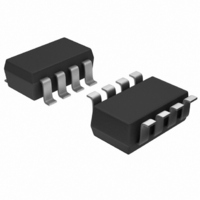
AD5273BRJ100-R2 Analog Devices Inc, AD5273BRJ100-R2 Datasheet - Page 5

AD5273BRJ100-R2
Manufacturer Part Number
AD5273BRJ100-R2
Description
IC DGTL POT 100K 64POS SOT23-8
Manufacturer
Analog Devices Inc
Datasheet
1.AD5273BRJZ10-R7.pdf
(24 pages)
Specifications of AD5273BRJ100-R2
Rohs Status
RoHS non-compliant
Taps
64
Resistance (ohms)
100K
Number Of Circuits
1
Temperature Coefficient
300 ppm/°C Typical
Memory Type
Non-Volatile
Interface
I²C, 2-Wire Serial
Voltage - Supply
2.7 V ~ 5.5 V
Operating Temperature
-40°C ~ 105°C
Mounting Type
Surface Mount
Package / Case
SOT-23-8
Resistance In Ohms
100K
Number Of Elements
1
# Of Taps
64
Resistance (max)
100KOhm
Power Supply Requirement
Single
Interface Type
Serial (2-Wire/I2C)
Single Supply Voltage (typ)
5V
Dual Supply Voltage (typ)
Not RequiredV
Single Supply Voltage (min)
2.7V
Single Supply Voltage (max)
5.5V
Dual Supply Voltage (min)
Not RequiredV
Dual Supply Voltage (max)
Not RequiredV
Operating Temp Range
-40C to 105C
Operating Temperature Classification
Industrial
Mounting
Surface Mount
Pin Count
8
For Use With
AD5273EVAL - BOARD EVAL FOR AD5273
Lead Free Status / RoHS Status
Not Compliant
Other names
AD5273BRJ100-R2TR
Parameter
DYNAMIC CHARACTERISTICS
INTERFACE TIMING CHARACTERISTICS
1
2
3
4
5
6
7
8
9
10
11
12
13
14
15
Typical values represent average readings at 25°C, V
Resistor position nonlinearity error, R-INL, is the deviation from an ideal value measured between the maximum resistance and the minimum resistance wiper
positions. R-DNL measures the relative step change from ideal between successive tap positions. Parts are guaranteed monotonic.
V
∆R
INL and DNL are measured at V
potentiometer divider similar to a voltage output DAC. V
conditions.
The A, B, and W resistor terminals have no limitations on polarity with respect to each other.
Guaranteed by design; not subject to production test.
The minimum voltage requirement on the V
However, care must be taken to ensure that the minimum V
Different from the operating power supply; the power supply for OTP is used one time only.
Different from the operating current; the supply current for OTP lasts approximately 400 ms for the one time it is needed.
See Figure 28 for the energy plot during the OTP program.
P
Bandwidth, noise, and settling time depend on the terminal resistance value chosen. The lowest R value results in the fastest settling time and highest bandwidth.
All dynamic characteristics use V
See Figure 29 for the location of the measured values.
The highest R value results in the minimum overall power consumption.
AB
Power Dissipation
Power Supply Sensitivity
Bandwidth, −3 dB
Total Harmonic Distortion
Adjustment Settling Time
Power-Up Settling Time—
Resistor Noise Voltage
SCL Clock Frequency
t
t
t
t
t
t
t
t
t
t
OTP Program Time
DISS
BUF
HD; STA
LOW
HIGH
SU; STA
HD; DAT
SU; DAT
F
R
SU; STO
WB
= V
Fall Time of Both SDA and
Rise Time of Both SDA and
After Fuses Blown
Stop and Start
(Repeated Start)
Start Condition
SCL Signals
SCL Signals
/∆T = ∆R
is calculated from (I
Bus Free Time Between
Low Period of SCL Clock
DD
High Period of SCL Clock
Setup Time for
, wiper (V
Hold Time
Data Setup Time
Setup Time for Stop Condition
Data Hold Time
WA
/∆T. Temperature coefficient is code-dependent; see the Typical Performance Characteristics section.
W
) = no connect.
12
DD
× V
DD
W
. INL with the RDAC configured as a potentiometer divider similar to a voltage output DAC. V
). CMOS logic level inputs result in minimum power dissipation.
DD
7, 13, 14
= 5 V.
7, 14, 15
IH
is 0.7 × V
DD
Symbol
P
PSRR
PSRR
BW_1 kΩ
BW_10 kΩ
BW_50 kΩ
BW_100 kΩ
THD
t
t
e
f
t
t
t
t
t
t
t
t
t
t
t
SCL
S1
S2
1
2
3
4
5
6
7
8
9
10
11
N_WB
DISS
= 5 V, and V
DD
A
. For example, V
W
= V
IH
DD
is met when the SCL and SDA are driven directly from a low voltage logic controller without pull-up resistors.
and V
SS
= 0 V.
B
= 0 V. DNL specification limits of ±1 LSB maximum are guaranteed monotonic operating
Test Conditions/Comments
V
R
R
R
R
R
R
V
f = 1 kHz
V
V
V
V
R
Applies to all parts
After this period, the first clock
pulse is generated
IH
Rev. H | Page 5 of 24
AB
IH
AB
AB
AB
AB
AB
AB
A
A
B
A
B
min = 3.5 V when V
= 0 V, measured at V
= 0 V, measured at V
= 1 V rms, R
= 5 V ± 1 LSB error band,
= 5 V ± 1 LSB error band,
= 5 V or V
= 1 kΩ, f = 1 kHz, code = 0x20
= 1 kΩ
= 10 kΩ, 50 kΩ, 100 kΩ
= 1 kΩ, code = 0x20
= 10 kΩ, code = 0x20
= 50 kΩ, code = 0x20
= 100 kΩ, code = 0x20
IL
= 0 V, V
AB
= 1 kΩ, V
DD
= 5 V. It is typical for the SCL and SDA resistors to be pulled up to V
DD
W
, V
W
= 5 V
DD
B
= 0 V,
= 5 V
Min
−0.3
−0.05
1.3
0.6
1.3
0.6
0.6
0.1
0.6
W
with the RDAC configured as a
Typ
6000
600
110
60
0.05
5
5
3
400
0.5
1
Max
27.5
+0.3
+0.05
400
50
0.9
0.3
0.3
AD5273
Unit
μW
%/%
kHz
kHz
kHz
kHz
%
μs
μs
kHz
μs
μs
μs
μs
μs
μs
μs
μs
μs
μs
ms
%/%
nV/√Hz
DD
.


