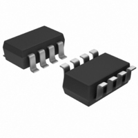
AD5273BRJ50-R2 Analog Devices Inc, AD5273BRJ50-R2 Datasheet - Page 7

AD5273BRJ50-R2
Manufacturer Part Number
AD5273BRJ50-R2
Description
IC DGTL POT 50K 64POS SOT23-8
Manufacturer
Analog Devices Inc
Datasheet
1.AD5273BRJZ10-R7.pdf
(24 pages)
Specifications of AD5273BRJ50-R2
Rohs Status
RoHS non-compliant
Taps
64
Resistance (ohms)
50K
Number Of Circuits
1
Temperature Coefficient
300 ppm/°C Typical
Memory Type
Non-Volatile
Interface
I²C, 2-Wire Serial
Voltage - Supply
2.7 V ~ 5.5 V
Operating Temperature
-40°C ~ 105°C
Mounting Type
Surface Mount
Package / Case
SOT-23-8
Resistance In Ohms
50K
For Use With
AD5273EVAL - BOARD EVAL FOR AD5273
Other names
AD5273BRJ50-R2
AD5273BRJ50-R2TR
AD5273BRJ50-R2TR
PIN CONFIGURATION AND FUNCTION DESCRIPTIONS
Table 3. Pin Function Descriptions
Pin No.
1
2
3
4
5
6
7
8
W
B
A
Mnemonic
V
GND
SCL
SDA
AD0
DD
Description
Wiper Terminal W. GND ≤ V
Positive Power Supply. Specified for non-OTP operation from 2.7 V to 5.5 V. For OTP programming, V
must be set within the window of 5 V to 5.5 V for the 1 kΩ (DD8) and 10 kΩ (DD9) options, or within the
window of 4.75 V to 5.25 V for the 50 kΩ (DYG) and 100 kΩ (DYH) options, and be capable of sourcing 100 mA.
Common Ground.
Serial Clock Input. Requires a pull-up resistor. If it is driven directly from a logic controller without the pull-up
resistor, ensure that the V
Serial Data Input/Output. Requires a pull-up resistor. If it is driven directly from a logic controller without the
pull-up resistor, ensure that the V
I
Resistor Terminal B. GND ≤ V
Resistor Terminal A. GND ≤ V
2
C Device Address Bit. Allows a maximum of two AD5273 devices to be addressed.
IH
GND
SCL
V
W
minimum is 0.7 × V
DD
W
Figure 2. Pin Configuration
B
A
≤ V
≤ V
≤ V
1
2
3
4
Rev. H | Page 7 of 24
DD
DD
(Not to Scale)
IH
DD
.
AD5273
TOP VIEW
minimum is 0.7 × V
.
.
8
7
6
5
DD
A
B
AD0
SDA
.
DD
.
AD5273
DD_OTP


