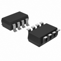
AD5273BRJ50-R2 Analog Devices Inc, AD5273BRJ50-R2 Datasheet - Page 17

AD5273BRJ50-R2
Manufacturer Part Number
AD5273BRJ50-R2
Description
IC DGTL POT 50K 64POS SOT23-8
Manufacturer
Analog Devices Inc
Datasheet
1.AD5273BRJZ10-R7.pdf
(24 pages)
Specifications of AD5273BRJ50-R2
Rohs Status
RoHS non-compliant
Taps
64
Resistance (ohms)
50K
Number Of Circuits
1
Temperature Coefficient
300 ppm/°C Typical
Memory Type
Non-Volatile
Interface
I²C, 2-Wire Serial
Voltage - Supply
2.7 V ~ 5.5 V
Operating Temperature
-40°C ~ 105°C
Mounting Type
Surface Mount
Package / Case
SOT-23-8
Resistance In Ohms
50K
For Use With
AD5273EVAL - BOARD EVAL FOR AD5273
Other names
AD5273BRJ50-R2
AD5273BRJ50-R2TR
AD5273BRJ50-R2TR
I
Write Bit Patterns
Read Bit Pattern
For users who do not use the software solution, the AD5273 can
be controlled via an I
to this bus as a slave device. Referring to Figure 42, Figure 43,
and Figure 44, the 2-wire I
follows:
1.
2
C CONTROLLER PROGRAMMING
The master initiates data transfer by establishing a start
condition. A start condition is defined as a high-to-low
transition on the SDA line while SCL is high, as shown in
Figure 42. The byte following the start condition is the
slave address byte, which consists of six MSBs defined as
010110. The next bit is AD0; it is an I
Depending on the states of the AD0 bits, two AD5273s can
be addressed on the same bus, as shown in Figure 45. The
last LSB is the R/ W bit, which determines whether data is
read from or written to the slave device.
The slave address corresponding to the transmitted address
responds by pulling the SDA line low during the ninth
clock pulse (this is termed the acknowledge bit). At this
stage, all other devices on the bus remain idle while the
selected device waits for data to be written to or read from
its serial register.
START BY
START BY
MASTER
MASTER
SCL
SDA
SCL
SDA
0
0
0
0
2
C-compatible serial bus and is connected
START BY
1
1
SLAVE ADDRESS BYTE
SLAVE ADDRESS BYTE
MASTER
0
0
2
C serial bus protocol operates as
SCL
SDA
FRAME 1
FRAME 1
1
1
1
1
0
0
0
0
1
AD0 R/W
AD0 R/W
SLAVE ADDRESS BYTE
2
C device address bit.
0
ACK. BY
ACK. BY
FRAME 1
AD5273
AD5273
1
Figure 44. Reading Data from the RDAC Register
8
8
Figure 43. Activating One-Time Programming
1
Figure 42. Writing to the RDAC Register
0
0
0
1
0
X
X
AD0 R/W
Rev. H | Page 17 of 24
X
X
INSTRUCTION BYTE
INSTRUCTION BYTE
X
X
ACK. BY
FRAME 2
FRAME 2
AD5273
8
X
X
E1
0
X
X
2.
3.
E0
DATA BYTE FROM SELECTED
X
X
D5
A write operation contains one more instruction byte than
the read operation. The instruction byte in the write mode
follows the slave address byte. The MSB of the instruction
byte labeled T is the OTP bit. After acknowledging the
instruction byte, the last byte in the write mode is the data
byte. Data is transmitted over the serial bus in sequences of
nine clock pulses (eight data bits followed by an acknowl-
edge bit). The transitions on the SDA line must occur during
the low period of SCL and remain stable during the high
period of SCL, as shown in Figure 42.
In read mode, the data byte follows immediately after the
acknowledgment of the slave address byte. Data is trans-
mitted over the serial bus in sequences of nine clock pulses
(slight difference from write mode, there are eight data bits
followed by a no acknowledge bit). Similarly, the transitions
on the SDA line must occur during the low period of SCL
and remain stable during the high period of SCL, as shown
in Figure 44.
RDAC REGISTER
X
X
D4
ACK. BY
ACK. BY
AD5273
AD5273
FRAME 2
8
8
D3
0
X
0
X
D2
X
X
D1
D5
D5
NO ACK. BY
D0
AD5273
D4
D4
DATA BYTE
DATA BYTE
FRAME 1
FRAME 1
8
D3
D3
STOP BY
MASTER
D2
D2
D1
D1
D0
D0
ACK. BY
ACK. BY
AD5273
AD5273
8
8
STOP BY
MASTER
STOP BY
MASTER
AD5273


