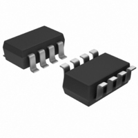
AD5273BRJ50-R2 Analog Devices Inc, AD5273BRJ50-R2 Datasheet - Page 5

AD5273BRJ50-R2
Manufacturer Part Number
AD5273BRJ50-R2
Description
IC DGTL POT 50K 64POS SOT23-8
Manufacturer
Analog Devices Inc
Datasheet
1.AD5273BRJZ10-R7.pdf
(24 pages)
Specifications of AD5273BRJ50-R2
Rohs Status
RoHS non-compliant
Taps
64
Resistance (ohms)
50K
Number Of Circuits
1
Temperature Coefficient
300 ppm/°C Typical
Memory Type
Non-Volatile
Interface
I²C, 2-Wire Serial
Voltage - Supply
2.7 V ~ 5.5 V
Operating Temperature
-40°C ~ 105°C
Mounting Type
Surface Mount
Package / Case
SOT-23-8
Resistance In Ohms
50K
For Use With
AD5273EVAL - BOARD EVAL FOR AD5273
Other names
AD5273BRJ50-R2
AD5273BRJ50-R2TR
AD5273BRJ50-R2TR
Parameter
DYNAMIC CHARACTERISTICS
INTERFACE TIMING CHARACTERISTICS
1
2
3
4
5
6
7
8
9
10
11
12
13
14
15
Typical values represent average readings at 25°C, V
Resistor position nonlinearity error, R-INL, is the deviation from an ideal value measured between the maximum resistance and the minimum resistance wiper
positions. R-DNL measures the relative step change from ideal between successive tap positions. Parts are guaranteed monotonic.
V
∆R
INL and DNL are measured at V
potentiometer divider similar to a voltage output DAC. V
conditions.
The A, B, and W resistor terminals have no limitations on polarity with respect to each other.
Guaranteed by design; not subject to production test.
The minimum voltage requirement on the V
However, care must be taken to ensure that the minimum V
Different from the operating power supply; the power supply for OTP is used one time only.
Different from the operating current; the supply current for OTP lasts approximately 400 ms for the one time it is needed.
See Figure 28 for the energy plot during the OTP program.
P
Bandwidth, noise, and settling time depend on the terminal resistance value chosen. The lowest R value results in the fastest settling time and highest bandwidth.
All dynamic characteristics use V
See Figure 29 for the location of the measured values.
The highest R value results in the minimum overall power consumption.
AB
Power Dissipation
Power Supply Sensitivity
Bandwidth, −3 dB
Total Harmonic Distortion
Adjustment Settling Time
Power-Up Settling Time—
Resistor Noise Voltage
SCL Clock Frequency
t
t
t
t
t
t
t
t
t
t
OTP Program Time
DISS
BUF
HD; STA
LOW
HIGH
SU; STA
HD; DAT
SU; DAT
F
R
SU; STO
WB
= V
Fall Time of Both SDA and
Rise Time of Both SDA and
After Fuses Blown
Stop and Start
(Repeated Start)
Start Condition
SCL Signals
SCL Signals
/∆T = ∆R
is calculated from (I
Bus Free Time Between
Low Period of SCL Clock
DD
High Period of SCL Clock
Setup Time for
, wiper (V
Hold Time
Data Setup Time
Setup Time for Stop Condition
Data Hold Time
WA
/∆T. Temperature coefficient is code-dependent; see the Typical Performance Characteristics section.
W
) = no connect.
12
DD
× V
DD
W
. INL with the RDAC configured as a potentiometer divider similar to a voltage output DAC. V
). CMOS logic level inputs result in minimum power dissipation.
DD
7, 13, 14
= 5 V.
7, 14, 15
IH
is 0.7 × V
DD
Symbol
P
PSRR
PSRR
BW_1 kΩ
BW_10 kΩ
BW_50 kΩ
BW_100 kΩ
THD
t
t
e
f
t
t
t
t
t
t
t
t
t
t
t
SCL
S1
S2
1
2
3
4
5
6
7
8
9
10
11
N_WB
DISS
= 5 V, and V
DD
A
. For example, V
W
= V
IH
DD
is met when the SCL and SDA are driven directly from a low voltage logic controller without pull-up resistors.
and V
SS
= 0 V.
B
= 0 V. DNL specification limits of ±1 LSB maximum are guaranteed monotonic operating
Test Conditions/Comments
V
R
R
R
R
R
R
V
f = 1 kHz
V
V
V
V
R
Applies to all parts
After this period, the first clock
pulse is generated
IH
Rev. H | Page 5 of 24
AB
IH
AB
AB
AB
AB
AB
AB
A
A
B
A
B
min = 3.5 V when V
= 0 V, measured at V
= 0 V, measured at V
= 1 V rms, R
= 5 V ± 1 LSB error band,
= 5 V ± 1 LSB error band,
= 5 V or V
= 1 kΩ, f = 1 kHz, code = 0x20
= 1 kΩ
= 10 kΩ, 50 kΩ, 100 kΩ
= 1 kΩ, code = 0x20
= 10 kΩ, code = 0x20
= 50 kΩ, code = 0x20
= 100 kΩ, code = 0x20
IL
= 0 V, V
AB
= 1 kΩ, V
DD
= 5 V. It is typical for the SCL and SDA resistors to be pulled up to V
DD
W
, V
W
= 5 V
DD
B
= 0 V,
= 5 V
Min
−0.3
−0.05
1.3
0.6
1.3
0.6
0.6
0.1
0.6
W
with the RDAC configured as a
Typ
6000
600
110
60
0.05
5
5
3
400
0.5
1
Max
27.5
+0.3
+0.05
400
50
0.9
0.3
0.3
AD5273
Unit
μW
%/%
kHz
kHz
kHz
kHz
%
μs
μs
kHz
μs
μs
μs
μs
μs
μs
μs
μs
μs
μs
ms
%/%
nV/√Hz
DD
.


