ADC12451CIJ National Semiconductor, ADC12451CIJ Datasheet - Page 15

ADC12451CIJ
Manufacturer Part Number
ADC12451CIJ
Description
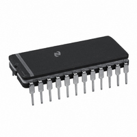
IC ADC 12BIT DYNAM TEST 24CDIP
Manufacturer
National Semiconductor
Datasheet
1.ADC12451CIJ.pdf
(18 pages)
Specifications of ADC12451CIJ
Number Of Bits
12
Sampling Rate (per Second)
83k
Data Interface
Parallel
Number Of Converters
2
Power Dissipation (max)
113mW
Voltage Supply Source
Analog and Digital, Dual ±
Operating Temperature
-40°C ~ 85°C
Mounting Type
Through Hole
Package / Case
24-CDIP (0.600", 15.24mm)
Lead Free Status / RoHS Status
Contains lead / RoHS non-compliant
Other names
*ADC12451CIJ
Available stocks
Company
Part Number
Manufacturer
Quantity
Price
3 0 Analog Considerations
3 5 INPUT BYPASS CAPACITORS
An external capacitor can be used to filter out any noise due
to inductive pickup by a long input lead and will not degrade
the accuracy of the conversion result
3 6 INPUT SOURCE RESISTANCE
The analog input can be modeled as shown in Figure 6
External R
voltage on C
input voltage With t
analog input voltage to settle properly
3 7 POWER SUPPLIES
Noise spikes on the V
conversion errors as the comparator will respond to this
noise The A D is especially sensitive during the Auto-Zero
or -Cal procedures to any power supply spikes Low induc-
tance tantalum capacitors of 10
with 0 1 F ceramic capacitors are recommended for supply
bypassing Separate bypass capacitors should be placed
close to the DV
voltage source is available in the system a separate
LM340LAZ-5 0 voltage regulator for the A-to-D’s V
other analog circuitry) will greatly reduce digital noise on the
supply line
3 8 THE CALIBRATION CYCLE
On power up the ADC12451 goes through an Auto-Cal cy-
cle which cannot be interrupted Since the power supply
reference and clock will not be stable at power up this first
calibration cycle will not result in an accurate calibration of
the A D A new calibration cycle needs to be started after
the power supplies reference and clock have been given
enough time to stabilize During the calibration cycle cor-
rection values are determined for the offset voltage of the
sampled data comparator and any linearity and gain errors
These values are stored in internal RAM and used during an
analog-to-digital conversion to bring the overall full-scale
offset and linearity errors down to the specified limits Full-
scale error typically changes
and linearity error changes even less therefore it should be
necessary to go through the calibration cycle only once af-
ter power up if Auto-Zero is used to correct the zero error
S
will lengthen the time period necessary for the
REF
CC
to settle to within
A
AV
e
CC
CC
3 5 s R
and V
and V
g
0 2 LSB over temperature
b
b
S s
supply lines can cause
F or greater paralleled
pins If an unregulated
1 k
LSB of the analog
FIGURE 6 Analog Input Equivalent Circuit
(Continued)
will allow a 5V
CC
(and
15
change Since Auto-Zero cannot be activated with S H con-
version method it may be necessary to do a calibration cy-
cle more than once
3 9 THE AUTO-ZERO CYCLE
To correct for any change in the zero (offset) error of the
A D the auto-zero cycle can be used It may be necessary
to do an auto-zero cycle whenever the ambient temperature
changes significantly (See the curve titled ‘‘Zero Error
Change vs Ambient Temperature’’ in the Typical Perform-
ance Characteristics ) A change in the ambient temperature
will cause the V
change which may cause the zero error of the A D to be
greater than
tain the zero error to
4 0 Dynamic Performance
Many applications require the A D converter to digitize ac
signals but the standard dc integral and differential nonlin-
earity specifications will not accurately predict the A D con-
verter’s performance with ac input signals The important
specifications for ac applications reflect the converter’s abil-
ity to digitize ac signals without significant spectral errors
and without adding noise to the digitized signal Dynamic
characteristics such as signal-to-noise (S N) signal-to-
noise
bandwidth aperture time and aperture jitter are quantitative
measures of the A D converter’s capability
An A D converter’s ac performance can be measured using
Fast Fourier Transform (FFT) methods A sinusoidal wave-
form is applied to the A D converter’s input and the trans-
form is then performed on the digitized waveform S (N
and S N are calculated from the resulting FFT data and a
spectral plot may also be obtained Typical values for S N
are shown in the table of Electrical Characteristics and
spectral plots of S (N
formance curves
The A D converter’s noise and distortion levels will change
with the frequency of the input signal with more distortion
and noise occurring at higher signal frequencies This can
be seen in the S (N
curves will also give an indication of the full power band-
width (the frequency at which the S (N
3 dB)
a
distortion ratio (S (N
g
1 LSB An auto-zero cycle will typically main-
OS
a
of the sampled data comparator to
g
a
TL H 11025 – 23
D) versus frequency curves These
1 LSB or less
D) are included in the typical per-
a
D)) effective bits full power
a
D) or S N drops
a
D)


