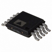
AD7992BRM-1 Analog Devices Inc, AD7992BRM-1 Datasheet - Page 6

AD7992BRM-1
Manufacturer Part Number
AD7992BRM-1
Description
IC ADC 12BIT 2CHAN I2C 10MSOP
Manufacturer
Analog Devices Inc
Datasheet
1.AD7992BRMZ-1.pdf
(28 pages)
Specifications of AD7992BRM-1
Number Of Bits
12
Sampling Rate (per Second)
79k
Data Interface
I²C, Serial
Number Of Converters
1
Power Dissipation (max)
2.2mW
Voltage Supply Source
Single Supply
Operating Temperature
-40°C ~ 125°C
Mounting Type
Surface Mount
Package / Case
10-TFSOP (0.118", 3.00mm Width)
For Use With
EVAL-AD7992CB - BOARD EVALUATION FOR AD7992
Lead Free Status / RoHS Status
Contains lead / RoHS non-compliant
AD7992
Parameter
t
t
t
t
t
t
1
2
10
11
11A
12
SP
POWER-UP
A device must provide a data hold time for SDA in order to bridge the undefined region of the SCL falling edge.
For 3 V supplies, the maximum hold time with
SDA
SCL
S = START CONDITION
P = STOP CONDITION
P
Conditions
Standard mode
Fast mode
High speed mode
Standard mode
Fast mode
High speed mode
Standard mode
Fast mode
High speed mode
Standard mode
Fast mode
High speed mode
Fast mode
High speed mode
t
7
C
C
C
C
C
C
C
C
S
B
B
B
B
B
B
B
B
= 100 pF max
= 400 pF max
= 100 pF max
= 400 pF max
= 100 pF max
= 400 pF max
= 100 pF max
= 400 pF max
t
6
t
2
t
11
t
4
C
0
1
Min
20 + 0.1 C
10
20
20 + 0.1 C
10
20
20 + 0.1 C
10
20
20 + 0.1 C
10
20
0
B
= 100 pF max is 100 ns max.
Figure 2. Two-Wire Serial Interface Timing Diagram
Limit at T
B
B
B
B
t
1
t
Max
300
300
80
160
1000
300
40
80
1000
300
80
160
300
300
40
80
50
10
12
MIN
t
3
Rev. 0 | Page 6 of 28
, T
MAX
Unit
ns
ns
ns
ns
ns
ns
ns
ns
ns
ns
ns
ns
ns
ns
ns
ns
ns
ns
µs typ
S
Description
t
t
t
condition and after an acknowledge bit
t
Pulse width of suppressed spike
Power-up time
FDA
RCL
RCL1
FCL
t
5
, rise time of SCL signal
, fall time of SCL signal
, fall time of SDA signal
t
, rise time of SCL signal after a repeated START
10
t
6
t
8
P
t
9


