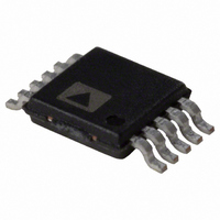
AD7992BRM-1 Analog Devices Inc, AD7992BRM-1 Datasheet - Page 21

AD7992BRM-1
Manufacturer Part Number
AD7992BRM-1
Description
IC ADC 12BIT 2CHAN I2C 10MSOP
Manufacturer
Analog Devices Inc
Datasheet
1.AD7992BRMZ-1.pdf
(28 pages)
Specifications of AD7992BRM-1
Number Of Bits
12
Sampling Rate (per Second)
79k
Data Interface
I²C, Serial
Number Of Converters
1
Power Dissipation (max)
2.2mW
Voltage Supply Source
Single Supply
Operating Temperature
-40°C ~ 125°C
Mounting Type
Surface Mount
Package / Case
10-TFSOP (0.118", 3.00mm Width)
For Use With
EVAL-AD7992CB - BOARD EVALUATION FOR AD7992
Lead Free Status / RoHS Status
Contains lead / RoHS non-compliant
WRITING TO THE AD7992
Depending on the register being written to, there are three
different writes for the AD7992.
WRITING TO THE ADDRESS POINTER REGISTER
FOR A SUBSEQUENT READ
In order to read from a particular register, the address pointer
register must first contain the address of that register. If it does
not, the correct address must be written to the address pointer
register by performing a single-byte write operation, as shown
in Figure 25. The write operation consists of the serial bus
address followed by the address pointer byte. No data is
written to any of the data registers. A read operation can be
subsequently performed to read the register of interest.
SDA
SCL
SDA
SCL
START BY
START BY
MASTER
MASTER
0
1
0
1
Figure 25. Writing to the Address Pointer Register to Select a Register for a Subsequent Read Operation
1
1
SERIAL BUS ADDRESS BYTE
SERIAL BUS ADDRESS BYTE
0
0
FRAME 1
A3
A3
FRAME 1
SCL (CONTINUED)
SDA (CONTINUED)
A2
A2
A1
A1
A0
Figure 26. Single-Byte Write Sequence
A0
R/W
R/W
Rev. 0 | Page 21 of 28
ACK. BY
ACK. BY
AD7992
AD7992
9
9
9
C4
1
C4
D7
1
1
C3
WRITING A SINGLE BYTE OF DATA TO THE ALERT
STATUS REGISTER, CYCLE REGISTER, OR
CONFIGURATION REGISTER
The alert status register, cycle register, and configuration
register are all 8-bit registers, so only one byte of data can be
written to each. Writing a single byte of data to one of these
registers consists of the serial bus write address, the chosen
data register address written to the address pointer register,
followed by the data byte written to the selected data register.
See Figure 26.
C3
D6
ADDRESS POINTER REGISTER BYTE
ADDRESS POINTER REGISTER BYTE
C2
C2
D5
C1
C1
D4
FRAME 2
DATA BYTE
FRAME 2
FRAME 3
P3
P3
D3
P2
P2
D2
P1
D1
P1
P0
P0
D0
ACK. BY
AD7992
ACK. BY
ACK. BY
AD7992
AD7992
9
9
9
STOP BY
MASTER
STOP BY
MASTER
AD7992


