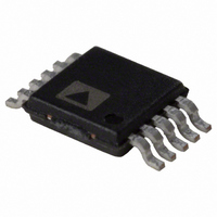
AD7992BRM-1 Analog Devices Inc, AD7992BRM-1 Datasheet - Page 19

AD7992BRM-1
Manufacturer Part Number
AD7992BRM-1
Description
IC ADC 12BIT 2CHAN I2C 10MSOP
Manufacturer
Analog Devices Inc
Datasheet
1.AD7992BRMZ-1.pdf
(28 pages)
Specifications of AD7992BRM-1
Number Of Bits
12
Sampling Rate (per Second)
79k
Data Interface
I²C, Serial
Number Of Converters
1
Power Dissipation (max)
2.2mW
Voltage Supply Source
Single Supply
Operating Temperature
-40°C ~ 125°C
Mounting Type
Surface Mount
Package / Case
10-TFSOP (0.118", 3.00mm Width)
For Use With
EVAL-AD7992CB - BOARD EVALUATION FOR AD7992
Lead Free Status / RoHS Status
Contains lead / RoHS non-compliant
Using the Limit Registers to Store Min/Max Conversion
Results
If full scale—that is, all 1s—is written to the hysteresis register
for a particular channel, the DATA
for that channel no longer act as limit registers as previously
described, but instead act as storage registers for the maximum
and minimum conversion results returned from conversions on
a channel over any given period of time. This function is useful
in applications where the widest span of actual conversion
results is required rather than using the ALERT to signal that an
intervention is necessary—for example, when monitoring
temperature extremes during refrigerated goods transportation.
Note that on power-up, the contents of the DATA
for each channel are full scale, while the contents of the
DATA
imum and maximum conversion values being stored in this
way are lost if power is removed or cycled.
ALERT STATUS REGISTER
The alert status register is an 8-bit read/write register that
provides information on an alert event. If a conversion results in
activating the ALERT pin or Alert_Flag bit in the conversion
result register (see the Limit Registers section) the alert status
register may be read to gain further information. It contains
two status bits per channel, one corresponding to each of the
DATA
where the violation occurred—that is, on which channel—and
whether the violation occurred on the upper or lower limit.
If a second alert event occurs on the other channel between
receiving the first alert and interrogating the alert status
register, the corresponding bit for that alert event is also set.
The entire contents of the alert status register can be cleared by
writing 1,1 to Bits D2 and D1 in the configuration register, as
shown in Table 11. This can also be achieved by writing all 1s to
the alert status register itself. Thus, if the alert status register is
addressed for a write operation, which is all 1s, the contents of
the alert status register are cleared or reset to all 0s.
Table 20. Alert Status Register
D7
0
Table 21. Alert Status Register Bit Function Descriptions
Bit
D0
D1
D2
D3
LOW
HIGH
Mnemonic
CH1LO
CH1HI
CH2LO
CH2HI
D6
0
registers are zero scale by default. Therefore, min-
and DATA
D5
0
Comment
Violation of DATA
bit is set to 1, no violation if bit is set to 0.
Violation of DATA
bit is set to 1, no violation if bit is set to 0.
Violation of DATA
bit is set to 1, no violation if bit is set to 0.
Violation of DATA
bit is set to 1, no violation if bit is set to 0.
LOW
D4
0
limits. The bit with a status of 1 shows
D3
CH2
HIGH
HI
LOW
HIGH
LOW
HIGH
and DATA
D2
CH2
limit on Channel 1 if
limit on Channel 2 if
limit on Channel 1 if
limit on Channel 2 if
LO
HIGH
LOW
D1
CH1
registers
register
HI
D0
CH1
Rev. 0 | Page 19 of 28
LO
CYCLE TIMER REGISTER
The cycle timer register is an 8-bit read/write register that stores
the conversion interval value for the automatic cycle mode of
the AD7992 (see the Modes of Operation section). The 5 MSBs
of the cycle timer register are unused and should contain 0s at
all times (see the Sample Delay and Bit Trial Delay section). On
power-up, the cycle timer register contains all 0s, thus disabling
automatic cycle operation of the AD7992. To enable automatic
cycle mode, the user must write to the cycle timer register,
selecting the required conversion interval. Table 22 shows the
structure of the cycle timer register, while Table 23 shows how
the bits in this register are decoded to provide various
automatic sampling intervals.
Table 22. Cycle Timer Register and Defaults at Power-Up
D7
Sample
Delay
0
Table 23. Cycle Timer Intervals
D2
0
0
0
0
1
1
1
1
SAMPLE DELAY AND BIT TRIAL DELAY
It is recommended that no I
conversion is taking place. However, this may not be possible,
for example, when operating in Mode 2 or the automatic cycle
mode. In order to maintain the performance of the ADC in
such cases, Bits D7 and D6 in the cycle timer register are used
to delay critical sample intervals and bit trials from occurring
while there is activity on the I
increasing the conversion time. When Bits D7 and D6 are both
0, the bit trial and sample interval delaying mechanism are
implemented. The default setting of D7 and D6 is 0. If bit trial
delays extend longer than 1 µs, the conversion terminates.
When D7 is 0, the sampling instant delay is implemented.
When D6 is 0, the bit trial delay is implemented. To turn off
both the sample delay and bit trial delay, set D7 and D6 to 1.
CYC Reg Value
D1
0
0
1
1
0
0
1
1
D6
Bit Trial
Delay
0
D0
0
1
0
1
0
1
0
1
D5
0
0
2
Mode not selected
T
T
T
T
T
T
T
Conversion Interval
(T
C bus activity occurs when a
2
CONVERT
CONVERT
CONVERT
CONVERT
CONVERT
CONVERT
CONVERT
C bus. This may have the effect of
D4
0
0
CONVERT
× 32
× 64
× 128
× 256
× 512
× 1024
× 2048
=conversion time of ADC)
D3
0
0
D2
Cyc
Bit 2
0
D1
Cyc
Bit 1
0
AD7992
D0
Cyc
Bit 0
0


