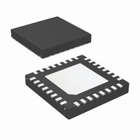
ADC14C080CISQ/NOPB National Semiconductor, ADC14C080CISQ/NOPB Datasheet - Page 7

ADC14C080CISQ/NOPB
Manufacturer Part Number
ADC14C080CISQ/NOPB
Description
ADC 14BIT 65/80MSPS 32-LLP
Manufacturer
National Semiconductor
Series
PowerWise®r
Datasheet
1.ADC14C080CISQENOPB.pdf
(24 pages)
Specifications of ADC14C080CISQ/NOPB
Number Of Bits
14
Sampling Rate (per Second)
80M
Data Interface
Parallel
Number Of Converters
1
Power Dissipation (max)
300mW
Voltage Supply Source
Single Supply
Operating Temperature
-40°C ~ 85°C
Mounting Type
Surface Mount
Package / Case
32-WFQFN Exposed Pad
Lead Free Status / RoHS Status
Lead free / RoHS Compliant
Other names
ADC14C080CISQ
Available stocks
Company
Part Number
Manufacturer
Quantity
Price
Company:
Part Number:
ADC14C080CISQ/NOPB
Manufacturer:
NS
Quantity:
6 218
DIGITAL OUTPUT CHARACTERISTICS (D0–D13, DRDY)
V
V
+I
−I
C
POWER SUPPLY CHARACTERISTICS
I
I
t
t
t
t
t
t
t
t
Symbol
A
DR
CH
CL
CONV
OD
SU
H
AD
AJ
OUT(1)
OUT(0)
Symb
OUT
SC
SC
ADC14C080 Timing and AC Characteristics
Unless otherwise specified, the following specifications apply: AGND = DRGND = 0V, V
+1.2V, f
measurements are taken at 50% of the signal amplitude. Boldface limits apply for T
T
A
= 25°C (Notes 8, 9)
CLK
Logical “1” Output Voltage
Logical “0” Output Voltage
Output Short Circuit Source Current
Output Short Circuit Sink Current
Digital Output Capacitance
Analog Supply Current
Digital Output Supply Current
Power Consumption
Power Down Power Consumption
Maximum Clock Frequency
Minimum Clock Frequency
Clock High Time
Clock Low Time
Conversion Latency
Output Delay of CLK to DATA
Data Output Setup Time
Data Output Hold Time
Aperture Delay
Aperture Jitter
= 80 MHz, 50% Duty Cycle, DCS Disabled, V
Parameter
Parameter
I
I
V
V
Full Operation
Full Operation (Note 12)
Excludes I
Clock disabled
OUT
OUT
Relative to rising edge of CLK (Note 13)
Relative to DRDY
Relative to DRDY
OUT
OUT
= −0.5 mA , V
= 1.6 mA, V
= 0V
= V
CM
DR
DR
= V
(Note 12)
CMO
7
Conditions
Conditions
DR
DR
, C
= 2.4V
L
= 2.4V
= 5 pF/pin. Typical values are for T
MIN
A
≤
= +3.0V, V
T
A
(Note 10)
(Note 10)
Typical
≤
Typical
5.5
6.5
0.6
0.1
−10
100
300
T
10
14
6
6
6
5
7
MAX
DR
. All other limits apply for
= +2.5V, Internal V
Limits
Limits
A
123
369
7.3
5.5
2.0
0.4
= 25°C. Timing
80
20
7
3
5
www.national.com
Clock Cycles
MHz (max)
MHz (min)
mW (max)
mA (max)
(Limits)
ns (min)
ns(max)
ns (min)
ns (min)
(Limits)
V (max)
V (min)
ps rms
Units
Units
mW
mA
mA
mA
REF
pF
ns
ns
ns
=


