ADC14C080CISQ/NOPB National Semiconductor, ADC14C080CISQ/NOPB Datasheet - Page 18
ADC14C080CISQ/NOPB
Manufacturer Part Number
ADC14C080CISQ/NOPB
Description
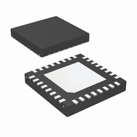
ADC 14BIT 65/80MSPS 32-LLP
Manufacturer
National Semiconductor
Series
PowerWise®r
Datasheet
1.ADC14C080CISQENOPB.pdf
(24 pages)
Specifications of ADC14C080CISQ/NOPB
Number Of Bits
14
Sampling Rate (per Second)
80M
Data Interface
Parallel
Number Of Converters
1
Power Dissipation (max)
300mW
Voltage Supply Source
Single Supply
Operating Temperature
-40°C ~ 85°C
Mounting Type
Surface Mount
Package / Case
32-WFQFN Exposed Pad
Lead Free Status / RoHS Status
Lead free / RoHS Compliant
Other names
ADC14C080CISQ
Available stocks
Company
Part Number
Manufacturer
Quantity
Price
Company:

Part Number:
ADC14C080CISQ/NOPB
Manufacturer:
NS
Quantity:
6 218


www.national.com
Functional Description
Operating on a single +3.0V supply, the ADC14C080 uses a
pipeline architecture and has error correction circuitry to help
ensure maximum performance. The differential analog input
signal is digitized to 14 bits. The user has the choice of using
an internal 1.2V stable reference, or using an external 1.2V
reference. Any external reference is buffered on-chip to ease
the task of driving that pin.
The output word rate is the same as the clock frequency. The
analog input is acquired at the rising edge of the clock and the
digital data for a given sample is delayed by the pipeline for
7 clock cycles. The digital outputs are CMOS compatible sig-
nals that are clocked by a synchronous data ready output
signal (DRDY, pin 21) at the same rate as the clock input. Duty
cycle stabilization and output data format are selectable using
the quad state function OF/DCS pin (pin 12). The output data
can be set for offset binary or two's complement.
Power-down is selectable using the PD pin (pin 30). A logic
high on the PD pin reduces the converter power consumption.
For normal operation, the PD pin should be connected to the
analog ground (AGND).
Applications Information
1.0 OPERATING CONDITIONS
We recommend that the following conditions be observed for
operation of the ADC14C080:
20 MHz
2.0 ANALOG INPUTS
2.1 Signal Inputs
2.1.1 Differential Analog Input Pins
The ADC14C080 has one pair of analog signal input pins,
V
signal, V
Figure 3shows the expected input signal range. Note that the
common mode input voltage, V
V
mode level for the analog input signal. The positive peaks of
the individual input signals should each never exceed 2.6V.
Each analog input pin of the differential pair should have a
maximum peak-to-peak voltage of 1V, be 180° out of phase
IN
CMO
2.7V
1.2V internal reference
V
V
+ and V
REF
CM
2.4V
(pin 32) for V
= 1.5V (from V
≤
= 1.2V (for an external reference)
≤
IN
V
≤
, is defined as
f
IN
A
CLK
V
−, which form a differential input pair. The input
≤
DR
≤
3.6V
≤
80 MHz
V
CM
V
A
CMO
IN
will ensure the proper input common
= (V
)
IN
+) – (V
CM
, should be 1.5V. Using
IN
−)
18
with each other and be centered around V
peak voltage swing at each analog input pin should not ex-
ceed the 1V or the output data will be clipped.
For single frequency sine waves the full scale error in LSB
can be described as approximately
Where dev is the angular difference in degrees between the
two signals having a 180° relative phase relationship to each
other (see Figure 4). For single frequency inputs, angular er-
rors result in a reduction of the effective full scale input. For
complex waveforms, however, angular errors will result in
distortion.
FIGURE 4. Angular Errors Between the Two Input Signals
It is recommended to drive the analog inputs with a source
impedance less than 100Ω. Matching the source impedance
for the differential inputs will improve even ordered harmonic
performance (particularly second harmonic).
Table 1indicates the input to output relationship of the AD-
C14C080.
Will Reduce the Output Level or Cause Distortion
FIGURE 3. Expected Input Signal Range
E
FS
= 16384 ( 1 - sin (90° + dev))
20209816
CM
20209815
.The peak-to-
Related parts for ADC14C080CISQ/NOPB
Image
Part Number
Description
Manufacturer
Datasheet
Request
R

Part Number:
Description:
National Semiconductor [8-Bit D/A Converter]
Manufacturer:
National Semiconductor
Datasheet:
Part Number:
Description:
National Semiconductor [Media Coprocessor]
Manufacturer:
National Semiconductor
Datasheet:
Part Number:
Description:
Digitally Controlled Tone and Volume Circuit with Stereo Audio Power Amplifier, Microphone Preamp Stage and National 3D Sound
Manufacturer:
National Semiconductor
Datasheet:
Part Number:
Description:
Digitally Controlled Tone and Volume Circuit with Stereo Audio Power Amplifier, Microphone Preamp Stage and National 3D Sound
Manufacturer:
National Semiconductor
Datasheet:
Part Number:
Description:
AC97 Rev 2 Codec with Sample Rate Conversion and National 3D Sound
Manufacturer:
National Semiconductor
Part Number:
Description:
Manufacturer:
National Semiconductor
Datasheet:
Part Number:
Description:
Manufacturer:
National Semiconductor
Datasheet:
Part Number:
Description:
General Purpose, Low Voltage, Low Power, Rail-to-Rail Output Operational Amplifiers
Manufacturer:
National Semiconductor
Datasheet:
Part Number:
Description:
8-bit 20 MSPS flash A/D converter.
Manufacturer:
National Semiconductor
Datasheet:
Part Number:
Description:
Low Noise Quad Operational Amplifier
Manufacturer:
National Semiconductor
Datasheet:
Part Number:
Description:
Quad Differential Line Receivers
Manufacturer:
National Semiconductor
Datasheet:
Part Number:
Description:
Quad High Speed Trapezoidal? Bus Transceiver
Manufacturer:
National Semiconductor
Datasheet:
Part Number:
Description:
Dual Line Receiver
Manufacturer:
National Semiconductor
Datasheet:
Part Number:
Description:
TTL to 10k ECL Level Translator with Latch
Manufacturer:
National Semiconductor
Datasheet: