ADC14C080CISQ/NOPB National Semiconductor, ADC14C080CISQ/NOPB Datasheet - Page 4
ADC14C080CISQ/NOPB
Manufacturer Part Number
ADC14C080CISQ/NOPB
Description
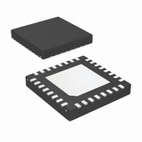
ADC 14BIT 65/80MSPS 32-LLP
Manufacturer
National Semiconductor
Series
PowerWise®r
Datasheet
1.ADC14C080CISQENOPB.pdf
(24 pages)
Specifications of ADC14C080CISQ/NOPB
Number Of Bits
14
Sampling Rate (per Second)
80M
Data Interface
Parallel
Number Of Converters
1
Power Dissipation (max)
300mW
Voltage Supply Source
Single Supply
Operating Temperature
-40°C ~ 85°C
Mounting Type
Surface Mount
Package / Case
32-WFQFN Exposed Pad
Lead Free Status / RoHS Status
Lead free / RoHS Compliant
Other names
ADC14C080CISQ
Available stocks
Company
Part Number
Manufacturer
Quantity
Price
Company:

Part Number:
ADC14C080CISQ/NOPB
Manufacturer:
NS
Quantity:
6 218


www.national.com
ANALOG POWER
Exposed Pad
DIGITAL POWER
Pin No.
3, 8, 10
4, 7, 9,
13-19,
23-29
21
20
22
Symbol
D0–D13
DRGND
DRDY
AGND
V
V
DR
A
Equivalent Circuit
4
Digital data output pins that make up the 14-bit conversion result.
D0 (pin 13) is the LSB, while D13 (pin 29) is the MSB of the output
word. Output levels are CMOS compatible.
Data Ready Strobe. The data output transition is synchronized with
the falling edge of this signal. This signal switches at the same
frequency as the CLK input.
Positive analog supply pins. These pins should be connected to a
quiet voltage source and be bypassed to AGND with 0.1 µF
capacitors located close to the power pins.
The ground return for the analog supply.
The exposed pad on back of package must be soldered to ground
plane to ensure rated performance.
Positive driver supply pin for the output drivers. This pin should be
connected to a quiet voltage source and be bypassed to DRGND
with a 0.1 µF capacitor located close to the power pin.
The ground return for the digital output driver supply. This pins
should be connected to the system digital ground, but not be
connected in close proximity to the ADC's AGND pins.
Description
Related parts for ADC14C080CISQ/NOPB
Image
Part Number
Description
Manufacturer
Datasheet
Request
R

Part Number:
Description:
National Semiconductor [8-Bit D/A Converter]
Manufacturer:
National Semiconductor
Datasheet:
Part Number:
Description:
National Semiconductor [Media Coprocessor]
Manufacturer:
National Semiconductor
Datasheet:
Part Number:
Description:
Digitally Controlled Tone and Volume Circuit with Stereo Audio Power Amplifier, Microphone Preamp Stage and National 3D Sound
Manufacturer:
National Semiconductor
Datasheet:
Part Number:
Description:
Digitally Controlled Tone and Volume Circuit with Stereo Audio Power Amplifier, Microphone Preamp Stage and National 3D Sound
Manufacturer:
National Semiconductor
Datasheet:
Part Number:
Description:
AC97 Rev 2 Codec with Sample Rate Conversion and National 3D Sound
Manufacturer:
National Semiconductor
Part Number:
Description:
Manufacturer:
National Semiconductor
Datasheet:
Part Number:
Description:
Manufacturer:
National Semiconductor
Datasheet:
Part Number:
Description:
General Purpose, Low Voltage, Low Power, Rail-to-Rail Output Operational Amplifiers
Manufacturer:
National Semiconductor
Datasheet:
Part Number:
Description:
8-bit 20 MSPS flash A/D converter.
Manufacturer:
National Semiconductor
Datasheet:
Part Number:
Description:
Low Noise Quad Operational Amplifier
Manufacturer:
National Semiconductor
Datasheet:
Part Number:
Description:
Quad Differential Line Receivers
Manufacturer:
National Semiconductor
Datasheet:
Part Number:
Description:
Quad High Speed Trapezoidal? Bus Transceiver
Manufacturer:
National Semiconductor
Datasheet:
Part Number:
Description:
Dual Line Receiver
Manufacturer:
National Semiconductor
Datasheet:
Part Number:
Description:
TTL to 10k ECL Level Translator with Latch
Manufacturer:
National Semiconductor
Datasheet: