ADC10154CIWMX/NOPB National Semiconductor, ADC10154CIWMX/NOPB Datasheet - Page 4
ADC10154CIWMX/NOPB
Manufacturer Part Number
ADC10154CIWMX/NOPB
Description
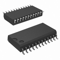
IC ADC 10BIT 24-SOIC
Manufacturer
National Semiconductor
Datasheet
1.ADC10158CIWMNOPB.pdf
(23 pages)
Specifications of ADC10154CIWMX/NOPB
Number Of Bits
10
Sampling Rate (per Second)
166k
Number Of Converters
1
Power Dissipation (max)
33mW
Voltage Supply Source
Analog and Digital, Dual ±
Operating Temperature
-65°C ~ 150°C
Mounting Type
Surface Mount
Package / Case
24-SOIC (0.300", 7.50mm Width)
Lead Free Status / RoHS Status
Lead free / RoHS Compliant
Other names
*ADC10154CIWMX
*ADC10154CIWMX/NOPB
ADC10154CIWMX
*ADC10154CIWMX/NOPB
ADC10154CIWMX
Available stocks
Company
Part Number
Manufacturer
Quantity
Price
Company:

Part Number:
ADC10154CIWMX/NOPB
Manufacturer:
NS
Quantity:
7 882


www.national.com
Symbol
DYNAMIC CONVERTER AND MULTIPLEXER CHARACTERISTICS
S/(N+D)
S/(N+D)
BIPOLAR CONVERTER AND MULTIPLEXER STATIC CHARACTERISTICS
UNIPOLAR AND BIPOLAR CONVERTER AND MULTIPLEXER STATIC CHARACTERISTICS
R
C
V
C
Symbol
The following specifications apply for V
operation or V
= T
Electrical Characteristics
The following specifications apply for V
operation or V
= T
AI
Electrical Characteristics
REF
REF
AI
J
J
= T
= T
MIN
MIN
Bipolar Negative Full-Scale
Error with Positive-Full
Scale Adjusted
Bipolar Offset Error
Bipolar Total Unadjusted
Error (Note 13)
Bipolar Power Supply
Sensitivity
Missing Codes
DC Common Mode
Error (Note 14)
Reference Input Resistance
Reference Input Capacitance
Analog Input Voltage
Analog Input Capacitance
Off Channel Leakage
Current
(Note 15)
Unipolar Signal-to-Noise+
Distortion Ratio
Bipolar Signal-to-Noise+
Distortion Ratio
to T
to T
−
−
= −5.0 V
= −5.0 V
MAX
MAX
; all other limits T
Parameter
Integral Linearity Error
Integral Linearity Error
; all other limits T
Parameter
DC
DC
Full-Scale Error
Full-Scale Error
for bipolar operation, and f
for bipolar operation, and f
Offset Error
Offset Error
Unipolar
Bipolar
A
+
A
+
= T
= AV
= T
= AV
(Continued)
J
J
= 25˚C. (Notes 8, 9, 12)
+
= 25˚C. (Notes 8, 9, 12)
+
V
V
V
V
V
V
V
V
+5.0V
+5.0V
On Channel = 5V
Off Channel = 0V
On Channel = 0V
Off Channel = 5V
= V
= DV
= DV
REF
REF
REF
+
REF
−
REF
IN
+
= +5V
= −5V
IN
f
f
f
f
IN
IN
IN
IN
+
+
+
+
+
= V
Conditions
+
+
where
= 5.0V
= 5.0V
= 5.0V
= 4.5V
= 4.5V
= 10 kHz, V
= 150 kHz, V
= 10 kHz, V
= 150 kHz, V
CLK
= + 5.0 V
CLK
= + 5.0 V
V
V
IN
IN
IN
±
±
−
= 5.0 MHz unless otherwise specified. Boldface limits apply for T
10%
10%
= 5.0 MHz unless otherwise specified. Boldface limits apply for T
−5.0V
0V
Conditions
4
DC
DC
IN
IN
, V
, V
IN
IN
= 4.85 V
=
REF
REF
= 4.85 V
=
±
±
4.85V
+
+
4.85V
(Note 10)
= 5.000 V
Typical
= 5.000 V
±
±
±
±
±
±
−400
±
±
400
p–p
0.25
0.25
0.25
0.25
0.25
0.25
70
30
0.5
0.5
7
p-p
DC
DC
, V
, V
(Note 10)
Typical
REF
CIN and CIWM
REF
60
58
60
58
(V
(V
(Note 11)
−
Suffixes
−
Limits
−1000
±
±
±
±
= GND, V
+
−
1000
±
±
±
±
= GND, V
4.5
9.5
+0.05)
−0.05)
1.25
±
0.75
0.75
0.75
2.5
2.5
1.5
0.5
0
3
(Note 11)
Limits
−
−
= GND for unipolar
= GND for unipolar
LSB (Max)
LSB (Max)
LSB (Max)
LSB (Max)
LSB (Max)
LSB (Max)
LSB (Max)
LSB (Max)
LSB (Max)
k
k
nA (Max)
nA (Max)
V (Max)
V (Min)
(Limit)
Units
LSB
LSB
(Limit)
pF
pF
Units
(Max)
(Max)
dB
dB
dB
dB
A
A
Related parts for ADC10154CIWMX/NOPB
Image
Part Number
Description
Manufacturer
Datasheet
Request
R

Part Number:
Description:
National Semiconductor [8-Bit D/A Converter]
Manufacturer:
National Semiconductor
Datasheet:
Part Number:
Description:
National Semiconductor [Media Coprocessor]
Manufacturer:
National Semiconductor
Datasheet:
Part Number:
Description:
Digitally Controlled Tone and Volume Circuit with Stereo Audio Power Amplifier, Microphone Preamp Stage and National 3D Sound
Manufacturer:
National Semiconductor
Datasheet:
Part Number:
Description:
Digitally Controlled Tone and Volume Circuit with Stereo Audio Power Amplifier, Microphone Preamp Stage and National 3D Sound
Manufacturer:
National Semiconductor
Datasheet:
Part Number:
Description:
AC97 Rev 2 Codec with Sample Rate Conversion and National 3D Sound
Manufacturer:
National Semiconductor
Part Number:
Description:
Manufacturer:
National Semiconductor
Datasheet:
Part Number:
Description:
Manufacturer:
National Semiconductor
Datasheet:
Part Number:
Description:
General Purpose, Low Voltage, Low Power, Rail-to-Rail Output Operational Amplifiers
Manufacturer:
National Semiconductor
Datasheet:
Part Number:
Description:
8-bit 20 MSPS flash A/D converter.
Manufacturer:
National Semiconductor
Datasheet:
Part Number:
Description:
Low Noise Quad Operational Amplifier
Manufacturer:
National Semiconductor
Datasheet:
Part Number:
Description:
Quad Differential Line Receivers
Manufacturer:
National Semiconductor
Datasheet:
Part Number:
Description:
Quad High Speed Trapezoidal? Bus Transceiver
Manufacturer:
National Semiconductor
Datasheet:
Part Number:
Description:
Dual Line Receiver
Manufacturer:
National Semiconductor
Datasheet:
Part Number:
Description:
TTL to 10k ECL Level Translator with Latch
Manufacturer:
National Semiconductor
Datasheet: