ADC10154CIWMX/NOPB National Semiconductor, ADC10154CIWMX/NOPB Datasheet - Page 16
ADC10154CIWMX/NOPB
Manufacturer Part Number
ADC10154CIWMX/NOPB
Description
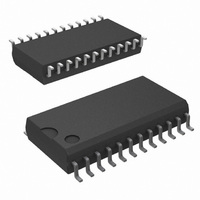
IC ADC 10BIT 24-SOIC
Manufacturer
National Semiconductor
Datasheet
1.ADC10158CIWMNOPB.pdf
(23 pages)
Specifications of ADC10154CIWMX/NOPB
Number Of Bits
10
Sampling Rate (per Second)
166k
Number Of Converters
1
Power Dissipation (max)
33mW
Voltage Supply Source
Analog and Digital, Dual ±
Operating Temperature
-65°C ~ 150°C
Mounting Type
Surface Mount
Package / Case
24-SOIC (0.300", 7.50mm Width)
Lead Free Status / RoHS Status
Lead free / RoHS Compliant
Other names
*ADC10154CIWMX
*ADC10154CIWMX/NOPB
ADC10154CIWMX
*ADC10154CIWMX/NOPB
ADC10154CIWMX
Available stocks
Company
Part Number
Manufacturer
Quantity
Price
Company:

Part Number:
ADC10154CIWMX/NOPB
Manufacturer:
NS
Quantity:
7 882


www.national.com
1.0 Functional Description
The ADC10154 and ADC10158 use successive approxima-
tion to digitize an analog input voltage. Additional logic has
been incorporated in the devices to allow for the program-
mability of the resolution, conversion time and digital output
format. A capacitive array and a resistive ladder structure are
used in the DAC portion of the A/D converters. The structure
of the DAC allows a very simple switching scheme to provide
a very versatile analog input multiplexer. Also, inherent in
this structure is a sample/hold. A 2.5V CMOS band-gap
reference is also provided on the ADC10154 and
ADC10158.
1.1 DIGITAL INTERFACE
The ADC10154 and ADC10158 have eight digital outputs
(DB0–DB8) and can be easily interfaced to an 8-bit data bus.
Taking CS and WR low simultaneously will strobe the data
word on the data-bus into the input latch. This word will be
decoded to determine the multiplexer channel selection, the
A/D conversion resolution and the output data format. The
following table shows the input word data-bit assignment.
DB0 through DB4 are assigned to the multiplexer address
data bits zero through four (MA0–MA4). Tables 2, 3 describe
the multiplexer address assignment. DB5 selects unsigned
or signed (U/S) operation. DB6 selects 8- or 10-bit resolu-
tion. DB7 selects left or right justification of the output data.
Refer to Table 1 for the effect the Control Input Data has on
the digital output word.
The conversion process is started by the rising edge of WR,
which sets the “start conversion” bit inside the ADC. If this bit
is set, the converter will start acquiring the input voltage on
the next falling edge of the internal CLK÷2 signal. The ac-
quisition period is 3 CLK÷2 periods, or 6 CLK periods. Im-
FIGURE 3. Starting a Conversion without Updating the Channel Configuration, Resolution, or Data Format
DS011225-44
16
mediately after the acquisition period the input signal is held
and the actual conversion begins. The number of clocks
required for a conversion is given in the following table:
Since the CLK÷2 signal is internal to the ADC, it is initially
impossible to know which falling edge of CLK corresponds to
the falling edge of CLK÷2. For the first conversion, the rising
edge of WR should occur at least t
edge of CLK. If this edge happens to be on the rising edge of
CLK÷2, this will add 2 CLK cycles to the total conversion
time. The phase of the CLK÷2 signal can be determined at
the end of the first conversion, when INT goes low. INT
always goes low on the falling edge of the CLK÷2 signal.
From the first falling edge of INT onward, every other falling
edge of CLK will correspond to the falling edge of CLK÷2.
With the phase of CLK÷2 now known, the conversion time
can be minimized by taking WR high at least t
the falling edge of CLK÷2.
Upon completion of the conversion, INT goes low to signal
the A/D conversion result is ready to be read. Taking CS and
RD low will enable the digital output buffer and put byte 1 of
the conversion result on DB0 through DB7. The falling edge
of RD resets the INT output high. Taking CS and RD low a
second time will put byte 2 of the conversion result on
DB7–DB0. Table 1 defines the DB0–DB7 assignment for
different Control Input Data. The second read does not have
to be completed before a new conversion is started.
Taking CS, WR and RD low simultaneously will start a con-
version without changing the multiplexer channel assign-
ment or output configuration and resolution. The timing dia-
gram in Figure 3 shows the sequence of events that
implement this function. Refer to Diagrams 1, 2, and 3 in the
Timing Diagrams section for the timing constraints that must
be met.
8-Bit
8-Bit + Sign
10-Bit
10-Bit + Sign
Conversion Type
CLK÷2
Cycles
WS
10
11
8
9
ns before any falling
Cycles (N)
DS011225-19
WS
CLK
16
18
20
22
ns before
Related parts for ADC10154CIWMX/NOPB
Image
Part Number
Description
Manufacturer
Datasheet
Request
R

Part Number:
Description:
National Semiconductor [8-Bit D/A Converter]
Manufacturer:
National Semiconductor
Datasheet:
Part Number:
Description:
National Semiconductor [Media Coprocessor]
Manufacturer:
National Semiconductor
Datasheet:
Part Number:
Description:
Digitally Controlled Tone and Volume Circuit with Stereo Audio Power Amplifier, Microphone Preamp Stage and National 3D Sound
Manufacturer:
National Semiconductor
Datasheet:
Part Number:
Description:
Digitally Controlled Tone and Volume Circuit with Stereo Audio Power Amplifier, Microphone Preamp Stage and National 3D Sound
Manufacturer:
National Semiconductor
Datasheet:
Part Number:
Description:
AC97 Rev 2 Codec with Sample Rate Conversion and National 3D Sound
Manufacturer:
National Semiconductor
Part Number:
Description:
Manufacturer:
National Semiconductor
Datasheet:
Part Number:
Description:
Manufacturer:
National Semiconductor
Datasheet:
Part Number:
Description:
General Purpose, Low Voltage, Low Power, Rail-to-Rail Output Operational Amplifiers
Manufacturer:
National Semiconductor
Datasheet:
Part Number:
Description:
8-bit 20 MSPS flash A/D converter.
Manufacturer:
National Semiconductor
Datasheet:
Part Number:
Description:
Low Noise Quad Operational Amplifier
Manufacturer:
National Semiconductor
Datasheet:
Part Number:
Description:
Quad Differential Line Receivers
Manufacturer:
National Semiconductor
Datasheet:
Part Number:
Description:
Quad High Speed Trapezoidal? Bus Transceiver
Manufacturer:
National Semiconductor
Datasheet:
Part Number:
Description:
Dual Line Receiver
Manufacturer:
National Semiconductor
Datasheet:
Part Number:
Description:
TTL to 10k ECL Level Translator with Latch
Manufacturer:
National Semiconductor
Datasheet: