ADC10154CIWMX/NOPB National Semiconductor, ADC10154CIWMX/NOPB Datasheet - Page 19

ADC10154CIWMX/NOPB
Manufacturer Part Number
ADC10154CIWMX/NOPB
Description
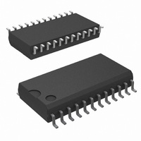
IC ADC 10BIT 24-SOIC
Manufacturer
National Semiconductor
Datasheet
1.ADC10158CIWMNOPB.pdf
(23 pages)
Specifications of ADC10154CIWMX/NOPB
Number Of Bits
10
Sampling Rate (per Second)
166k
Number Of Converters
1
Power Dissipation (max)
33mW
Voltage Supply Source
Analog and Digital, Dual ±
Operating Temperature
-65°C ~ 150°C
Mounting Type
Surface Mount
Package / Case
24-SOIC (0.300", 7.50mm Width)
Lead Free Status / RoHS Status
Lead free / RoHS Compliant
Other names
*ADC10154CIWMX
*ADC10154CIWMX/NOPB
ADC10154CIWMX
*ADC10154CIWMX/NOPB
ADC10154CIWMX
Available stocks
Company
Part Number
Manufacturer
Quantity
Price
Company:
Part Number:
ADC10154CIWMX/NOPB
Manufacturer:
NS
Quantity:
7 882
2.0 Applications Information
The minimum value of V
quite small (see Typical Performance Characteristics) to al-
low direct conversion of transducer outputs providing less
than a 5V output span. Particular care must be taken with
regard to noise pickup, circuit layout and system error volt-
age sources when operating with a reduced span due to the
increased sensitivity of the converter (1 LSB equals V
2
2.3 THE ANALOG INPUTS
Due to the sampling nature of the analog inputs, at the clock
edges short duration spikes of current will be seen on the
selected assigned negative input. Input bypass capacitors
should not be used if the source resistance is greater than
1 k
effective DC current to flow through the analog input source
resistance. An op amp RC active lowpass filter can provide
both impedance buffering and noise filtering should a high
impedance signal source be required. Bypass capacitors
may be used when the source impedance is very low without
any degradation in performance.
In a true differential input stage, a signal that is common to
both “+” and “−” inputs is cancelled. For the ADC10154 and
ADC10158, the positive input of a selected channel pair is
n
).
since they will average the AC current and cause an
REF
(V
REF
= V
REF
FIGURE 5. Different Reference Configurations
a. Ratiometric Using the Internal Reference
+
− V
b. Absolute Using a 4.096V Span
REF
(Continued)
−
) can be
REF
/
19
only sampled once before the start of a conversion during
the acquisition time (t
stable during the complete conversion sequence because it
is sampled before each decision in the SAR sequence.
Therefore, any AC common-mode signal present on the
analog inputs will not be completely cancelled and will cause
some conversion errors. For a sinusoid common-mode sig-
nal this error is:
V
where f
V
conversion time (t
For example, for a 60 Hz common-mode signal to generate
a
peak value would have to be approximately 731 mV.
2.4 OPTIONAL ADJUSTMENTS
2.4.1 Zero Error
The zero error of the A/D converter relates to the location of
the first riser of the transfer function (see Figure 1 ) and can
be measured by grounding the minus input and applying a
small magnitude positive or negative voltage to the plus
input. Zero error is the difference between actual DC input
error
PEAK
1
⁄
4
LSB error (1.24 mV) with a 4.5 µs conversion time, its
(Max) = V
is its peak voltage value, and t
CM
is the frequency of the common-mode signal,
DS011225-21
PEAK
C
= 22/f
(2 f
A
). The negative input needs to be
CM
DS011225-22
CLK
)(t
C
for 10-bit plus sign resolution).
)
C
is the A/D’s maximum
www.national.com


