ADC10154CIWMX/NOPB National Semiconductor, ADC10154CIWMX/NOPB Datasheet - Page 2
ADC10154CIWMX/NOPB
Manufacturer Part Number
ADC10154CIWMX/NOPB
Description
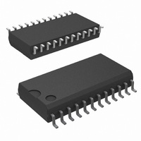
IC ADC 10BIT 24-SOIC
Manufacturer
National Semiconductor
Datasheet
1.ADC10158CIWMNOPB.pdf
(23 pages)
Specifications of ADC10154CIWMX/NOPB
Number Of Bits
10
Sampling Rate (per Second)
166k
Number Of Converters
1
Power Dissipation (max)
33mW
Voltage Supply Source
Analog and Digital, Dual ±
Operating Temperature
-65°C ~ 150°C
Mounting Type
Surface Mount
Package / Case
24-SOIC (0.300", 7.50mm Width)
Lead Free Status / RoHS Status
Lead free / RoHS Compliant
Other names
*ADC10154CIWMX
*ADC10154CIWMX/NOPB
ADC10154CIWMX
*ADC10154CIWMX/NOPB
ADC10154CIWMX
Available stocks
Company
Part Number
Manufacturer
Quantity
Price
Company:

Part Number:
ADC10154CIWMX/NOPB
Manufacturer:
NS
Quantity:
7 882


www.national.com
Connection Diagrams
Pin Descriptions
AV
DV
DGND
V
V
V
V
CS
−
REF
REF
REF
+
+
+
−
Out
,
Dual-in-Line and SO Packages
This is the positive analog supply. This pin
should be bypassed with a 0.1 µF ceramic ca-
pacitor and a 10 µF tantalum capacitor to the
system analog ground.
This is the positive digital supply. This supply
pin also needs to be bypassed with 0.1 µF
ceramic and 10 µF tantalum capacitors to the
system digital ground. AV
bypassed separately and tied to same power
supply.
This is the digital ground. All logic levels are
referred to this ground.
This is the negative analog supply. For unipolar
operation this pin may be tied to the system
analog ground or to a negative supply source.
It should not go above DGND by more than
50 mV. When bipolar operation is required, the
voltage on this pin will limit the analog input’s
negative voltage level. In bipolar operation this
supply pin needs to be bypassed with 0.1 µF
ceramic and 10 µF tantalum capacitors to the
system analog ground.
These are the positive and negative reference
inputs. The voltage difference between V
and V
span.
This is the internal band-gap voltage reference
output. For proper operation of the voltage ref-
erence, this pin needs to be bypassed with a
330 µF tantalum or electrolytic capacitor.
This is the chip select input. When a logic low
is applied to this pin the WR and RD pins are
enabled.
NS Package Number M24B
Order Number ADC10154
REF
−
Top View
will set the analog input voltage
+
and DV
DS011225-2
+
should be
REF
+
2
RD
WR
INT
CLK
DB0(MA0)
–DB7 (L/R)
CH0–CH7
Dual-in-Line and SO Packages
This is the read control input. When a logic low
is applied to this pin the digital outputs are
enabled and the INT output is reset high.
This is the write control input. The rising edge
of the signal applied to this pin selects the
multiplexer channel and initiates a conversion.
This is the interrupt output. A logic low at this
output indicates the completion of a conver-
sion.
This is the clock input. The clock frequency
directly controls the duration of the conversion
time (for example, in the 10-bit bipolar mode
t
6/f
These are the digital data inputs/outputs. DB0
is the least significant bit of the digital output
word; DB7 is the most significant bit in the
digital output word (see the Output Data Con-
figuration table). MA0 through MA4 are the
digital inputs for the multiplexer channel selec-
tion (see the Multiplexer Addressing tables).
U/S (Unsigned/Signed), 8/10, (8/10-bit resolu-
tion) and L/R (Left/Right justification) are the
digital input bits that set the A/D’s output word
format and resolution (see the Output Data
Configuration table). The conversion time is
modified by the chosen resolution (see Electri-
cal AC Characteristics table). The lower the
resolution, the faster the conversion will be.
These are the analog input multiplexer chan-
nels. They can be configured as single-ended
inputs,
pseudo-differential inputs (see the Multiplexer
Addressing tables for the input polarity
assignments).
C
CLK
= 22/f
Order Number ADC10158
NS Package Numbers
).
M28B or N28B
CLK
differential
Top View
) and the acquisition time (t
input
DS011225-3
pairs,
A
or
=
Related parts for ADC10154CIWMX/NOPB
Image
Part Number
Description
Manufacturer
Datasheet
Request
R

Part Number:
Description:
National Semiconductor [8-Bit D/A Converter]
Manufacturer:
National Semiconductor
Datasheet:
Part Number:
Description:
National Semiconductor [Media Coprocessor]
Manufacturer:
National Semiconductor
Datasheet:
Part Number:
Description:
Digitally Controlled Tone and Volume Circuit with Stereo Audio Power Amplifier, Microphone Preamp Stage and National 3D Sound
Manufacturer:
National Semiconductor
Datasheet:
Part Number:
Description:
Digitally Controlled Tone and Volume Circuit with Stereo Audio Power Amplifier, Microphone Preamp Stage and National 3D Sound
Manufacturer:
National Semiconductor
Datasheet:
Part Number:
Description:
AC97 Rev 2 Codec with Sample Rate Conversion and National 3D Sound
Manufacturer:
National Semiconductor
Part Number:
Description:
Manufacturer:
National Semiconductor
Datasheet:
Part Number:
Description:
Manufacturer:
National Semiconductor
Datasheet:
Part Number:
Description:
General Purpose, Low Voltage, Low Power, Rail-to-Rail Output Operational Amplifiers
Manufacturer:
National Semiconductor
Datasheet:
Part Number:
Description:
8-bit 20 MSPS flash A/D converter.
Manufacturer:
National Semiconductor
Datasheet:
Part Number:
Description:
Low Noise Quad Operational Amplifier
Manufacturer:
National Semiconductor
Datasheet:
Part Number:
Description:
Quad Differential Line Receivers
Manufacturer:
National Semiconductor
Datasheet:
Part Number:
Description:
Quad High Speed Trapezoidal? Bus Transceiver
Manufacturer:
National Semiconductor
Datasheet:
Part Number:
Description:
Dual Line Receiver
Manufacturer:
National Semiconductor
Datasheet:
Part Number:
Description:
TTL to 10k ECL Level Translator with Latch
Manufacturer:
National Semiconductor
Datasheet: