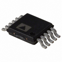
AD7982BRMZ Analog Devices Inc, AD7982BRMZ Datasheet - Page 13

AD7982BRMZ
Manufacturer Part Number
AD7982BRMZ
Description
IC ADC 18BIT 1MSPS PULSAR 10MSOP
Manufacturer
Analog Devices Inc
Series
PulSAR®r
Datasheet
1.AD7982BCPZ-RL.pdf
(24 pages)
Specifications of AD7982BRMZ
Data Interface
DSP, MICROWIRE™, QSPI™, Serial, SPI™
Design Resources
Converting a Single-Ended Signal with AD7982 Differential PulSAR ADC (CN0032) Precision Single-Supply Differential ADC Driver for Industrial-Level Signals (CN0180)
Number Of Bits
18
Sampling Rate (per Second)
1M
Number Of Converters
1
Power Dissipation (max)
8.6mW
Voltage Supply Source
Single Supply
Operating Temperature
-40°C ~ 85°C
Mounting Type
Surface Mount
Package / Case
10-TFSOP (0.118", 3.00mm Width)
Resolution (bits)
18bit
Sampling Rate
1MSPS
Input Channel Type
Differential
Supply Voltage Range - Analog
2.375V To 2.625V
Supply Current
350nA
Package
10MSOP
Resolution
18 Bit
Architecture
SAR
Number Of Analog Inputs
1
Digital Interface Type
Serial (3-Wire, 4-Wire, SPI, QSPI, Microwire)
Input Type
Voltage
Signal To Noise Ratio
98(Typ) dB
Polarity Of Input Voltage
Bipolar
Lead Free Status / RoHS Status
Lead free / RoHS Compliant
Available stocks
Company
Part Number
Manufacturer
Quantity
Price
Company:
Part Number:
AD7982BRMZ
Manufacturer:
ADI
Quantity:
1 000
Part Number:
AD7982BRMZ
Manufacturer:
ADI/亚德诺
Quantity:
20 000
Part Number:
AD7982BRMZ-REEL
Manufacturer:
ADI/亚德诺
Quantity:
20 000
Part Number:
AD7982BRMZ-REEL7
Manufacturer:
ADI/亚德诺
Quantity:
20 000
Company:
Part Number:
AD7982BRMZRL7
Manufacturer:
ADI
Quantity:
1 000
Company:
Part Number:
AD7982BRMZRL7
Manufacturer:
AD
Quantity:
1 234
Part Number:
AD7982BRMZRL7
Manufacturer:
ADI/亚德诺
Quantity:
20 000
Transfer Functions
The ideal transfer characteristic for the AD7982 is shown in
Figure 22 and Table 7.
100...010
100...001
100...000
011...110
011...101
011...111
–FSR + 0.5 LSB
–FSR
Figure 22. ADC Ideal Transfer Function
–FSR + 1 LSB
0 TO VREF
VREF TO 0
ADA4841
ANALOG INPUT
2, 3
+FSR – 1.5 LSB
V+
V–
V+
V–
V+
Figure 23. Typical Application Diagram with Multiple Supplies
NOTES
1
2
3
4
SEE VOLTAGE REFERENCE INPUT SECTION FOR REFERENCE SELECTION.
C
SEE DRIVER AMPLIFIER CHOICE SECTION.
OPTIONAL FILTER. SEE ANALOG INPUT SECTION.
SEE RECOMMENDED LAYOUT FIGURE 41 AND FIGURE 42.
+FSR – 1 LSB
REF
2.7nF
2.7nF
REF
4
4
20Ω
20Ω
IS USUALLY A 10µF CERAMIC CAPACITOR (X5R).
1
10µF
2
Rev. A | Page 13 of 24
IN+
IN–
GND
REF
AD7982
VDD
Table 7. Output Codes and Ideal Input Voltages
Description
FSR – 1 LSB
Midscale + 1 LSB
Midscale
Midscale – 1 LSB
–FSR + 1 LSB
–FSR
1
2
TYPICAL CONNECTION DIAGRAM
Figure 23 shows an example of the recommended connection
diagram for the AD7982 when multiple supplies are available.
This is also the code for an overranged analog input (V
This is also the code for an underranged analog input (V
VIO
SCK
SDO
CNV
SDI
100nF
100nF
3-WIRE INTERFACE
Analog Input
V
+4.999962 V
+38.15 μV
0 V
−38.15 μV
−4.999962 V
−5 V
REF
2.5V
1.8V TO 5V
= 5 V
IN+
Digital Output
Code (Hex)
0x1FFFF
0x00001
0x00000
0x3FFFF
0x20001
0x20000
− V
IN+
IN−
− V
above V
AD7982
IN−
1
2
below V
REF
− V
GND
GND
).
).


