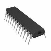
AD7710ANZ Analog Devices Inc, AD7710ANZ Datasheet - Page 27

AD7710ANZ
Manufacturer Part Number
AD7710ANZ
Description
IC ADC SIGNAL CONDITIONING 24DIP
Manufacturer
Analog Devices Inc
Datasheet
1.AD7710ARZ-REEL.pdf
(32 pages)
Specifications of AD7710ANZ
Data Interface
Serial
Number Of Bits
24
Sampling Rate (per Second)
1.03k
Number Of Converters
1
Power Dissipation (max)
45mW
Voltage Supply Source
Analog and Digital, Dual ±
Operating Temperature
-40°C ~ 85°C
Mounting Type
Through Hole
Package / Case
24-DIP (0.300", 7.62mm)
Resolution (bits)
24bit
Sampling Rate
1.02kSPS
Input Channel Type
Single Ended
Supply Voltage Range - Digital
4.75V To 5.25V
Supply Current
4.5mA
Digital Ic Case Style
DIP
Lead Free Status / RoHS Status
Lead free / RoHS Compliant
Available stocks
Company
Part Number
Manufacturer
Quantity
Price
Part Number:
AD7710ANZ
Manufacturer:
ADI/亚德诺
Quantity:
20 000
REV. G
APPLICATIONS
Figure 19 shows a strain gage interfaced directly to one of the
analog input channels of the AD7710. The differential inputs to
the AD7710 are connected directly to the bridge network of the
strain gage. In the diagram shown, the on-chip reference of the
AD7710 provides the voltage for the bridge network and also
provides the reference voltage for the AD7710. An alternative
scheme, outlined in Figure 20, shows the analog positive supply
voltage powering the bridge network and the AD7710, with the
R =
DUMMY
ACTIVE
GAGE
GAGE
I
EXCITATION
DUMMY
ACTIVE
V
GAGE
GAGE
Figure 20. Alternate Scheme for Generating AD7710 Reference Voltage
ANALOG SUPPLY
REF
R
R
EXCITATION
CURRENT
R
R
Figure 19. Strain-Gage Application with the AD7710
AIN1(+)
AIN1(–)
AIN2(+)
AIN2(–)
REF IN(+)
REF IN(–)
AIN1(+)
AIN1(–)
AIN2(+)
AIN2(–)
AGND
AGND
REFERENCE
OUT
REF
AD7710
2.5V
DGND
AD7710
DGND
IN(–)
REF
M
U
X
AV
V
DD
M
U
X
SS
V
–27–
PGA
SS
A = 1 – 128
PGA
RFS
A = 1 – 128
reference voltage for the AD7710 generated across a resistor
that is placed in series with the bridge network. In this case, the
value of the reference resistor is determined by the required
reference voltage divided by the value of the excitation current.
The on-chip PGA allows the AD7710 to handle an analog input
voltage range as low as 20 mV full scale. The differential inputs
of the part allow this analog input range to have an absolute
value anywhere between V
5V SUPPLY
RFS
DIGITAL
TFS
IN(+)
REGISTER
REF
CONTROL
TFS
DV
MODE SDATA SCLK
REGISTER
CONTROL
AUTO-ZEROED
CHARGE-BALANCING A/D
SERIAL INTERFACE
MODULATOR
DD
MODE SDATA SCLK
AUTO-ZEROED
CHARGE-BALANCING A/D
SERIAL INTERFACE
MODULATOR
V
CONVERTER
-
BIAS
V
CONVERTER
-
BIAS
GENERATION
REGISTER
OUTPUT
AV
CLOCK
GENERATION
REGISTER
DD
OUTPUT
DIGITAL
FILTER
5V SUPPLY
CLOCK
ANALOG
REFERENCE
DRDY
DIGITAL
FILTER
DRDY
2.5V
SS
DV
REF
OUT
A0
DD
and AV
A0
MCLK
I
MCLK
OUT
SYNC
N
DD
MCLK
IN
MCLK
OUT
SYNC
.
AD7710


